ZHCSGA6A February 2017 – June 2017 ADS114S06 , ADS114S08
PRODUCTION DATA.
- 1 特性
- 2 应用
- 3 说明
- 4 修订历史记录
- 5 Device Family Comparison Table
- 6 Pin Configuration and Functions
- 7 Specifications
- 8 Parameter Measurement Information
-
9 Detailed Description
- 9.1 Overview
- 9.2 Functional Block Diagram
- 9.3
Feature Description
- 9.3.1 Multiplexer
- 9.3.2 Low-Noise Programmable Gain Amplifier
- 9.3.3 Voltage Reference
- 9.3.4 Clock Source
- 9.3.5 Delta-Sigma Modulator
- 9.3.6 Digital Filter
- 9.3.7 Excitation Current Sources (IDACs)
- 9.3.8 Bias Voltage Generation
- 9.3.9 System Monitor
- 9.3.10 Status Register
- 9.3.11 General-Purpose Inputs and Outputs (GPIOs)
- 9.3.12 Low-Side Power Switch
- 9.3.13 Cyclic Redundancy Check (CRC)
- 9.3.14 Calibration
- 9.4 Device Functional Modes
- 9.5 Programming
- 9.6
Register Map
- 9.6.1
Configuration Registers
- 9.6.1.1 Device ID Register (address = 00h) [reset = xxh]
- 9.6.1.2 Device Status Register (address = 01h) [reset = 80h]
- 9.6.1.3 Input Multiplexer Register (address = 02h) [reset = 01h]
- 9.6.1.4 Gain Setting Register (address = 03h) [reset = 00h]
- 9.6.1.5 Data Rate Register (address = 04h) [reset = 14h]
- 9.6.1.6 Reference Control Register (address = 05h) [reset = 10h]
- 9.6.1.7 Excitation Current Register 1 (address = 06h) [reset = 00h]
- 9.6.1.8 Excitation Current Register 2 (address = 07h) [reset = FFh]
- 9.6.1.9 Sensor Biasing Register (address = 08h) [reset = 00h]
- 9.6.1.10 System Control Register (address = 09h) [reset = 10h]
- 9.6.1.11 Reserved Register (address = 0Ah) [reset = 00h]
- 9.6.1.12 Offset Calibration Register 1 (address = 0Bh) [reset = 00h]
- 9.6.1.13 Offset Calibration Register 2 (address = 0Ch) [reset = 00h]
- 9.6.1.14 Reserved Register (address = 0Dh) [reset = 00h]
- 9.6.1.15 Gain Calibration Register 1 (address = 0Eh) [reset = 00h]
- 9.6.1.16 Gain Calibration Register 2 (address = 0Fh) [reset = 40h]
- 9.6.1.17 GPIO Data Register (address = 10h) [reset = 00h]
- 9.6.1.18 GPIO Configuration Register (address = 11h) [reset = 00h]
- 9.6.1
Configuration Registers
- 10Application and Implementation
- 11Power Supply Recommendations
- 12Layout
- 13器件和文档支持
- 14机械、封装和可订购信息
7.7 Switching Characteristics
over operating ambient temperature range, DVDD = 2.7 V to 3.6 V, IOVDD = DVDD to 5.25 V, andDOUT/DRDY load = 20 pF || 100 kΩ to DGND (unless otherwise noted)
| PARAMETER | TEST CONDITIONS | MIN | TYP | MAX | UNIT(1) | |
|---|---|---|---|---|---|---|
| tp(CSDO) | Propagation delay time, CS falling edge to DOUT driven | 0 | 25 | ns | ||
| tp(SCDO) | Propagation delay time, SCLK rising edge to valid new DOUT | 3 | 30 | ns | ||
| tp(CSDOZ) | Propagation delay time, CS rising edge to DOUT high impedance | 0 | 25 | ns | ||
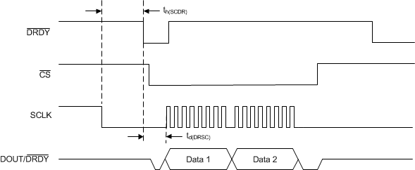
| tp(STDR) | Propagation delay time, START/SYNC rising edge (or first SCLK rising edge of any command or data read) to DRDY rising edge | 2 | tCLK | |||
| tw(DRH) | Pulse duration, DRDY high | 24 | tCLK | |||
| tp(GPIO) | Propagation delay time, last SCLK falling edge of WREG command to GPIOx output valid | 3 | 100 | ns | ||
| SPI timeout per 8 bit(2) | 215 | tCLK | ||||
(1) tCLK = 1 / fCLK
(2) The SPI interface resets when an entire byte is not sent within the specified timeout time.

NOTE:
Single-byte communication is shown. Actual communication can be multiple bytes.
NOTE:
Single-byte communication is shown. Actual communication can be multiple bytes. Figure 3. RESET Pin and RESET Command Timing Requirements
 Figure 4. START/SYNC Pin Timing Requirements
 Figure 5. START Command Timing Requirements
 Figure 6. Read Data Direct (Without an RDATA Command) Timing Requirements
 Figure 7. GPIO Switching Characteristics