TIDUES0E June 2019 – April 2024 TMS320F28P550SJ , TMS320F28P559SJ-Q1
- 1
- Description
- Resources
- Features
- Applications
- 6
- 1System Description
- 2System Overview
- 3Circuit Description
- 4Hardware, Software, Testing Requirements, and Test Results
- 5Design Files
- 6Related Documentation
- 7Terminology
- 8About the Author
- 9Revision History
4.4.1 Lab 1
Compile the project by selecting Lab 1: Open Loop PWM in the drop-down menu of Project Options from PowerSUITE GUI. This lab is intended to validate the PWM outputs and can be checked directly using the TIDA-010054 hardware (HW) or using the F2804X control card with a docking station.
Run the project by clicking the green run button in CCS.
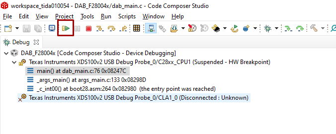 Figure 4-10 Run CCS
Populate the required variables in the watch window by loading JavaScript® setupdebugenv_lab1.js in the scripting console.
 Figure 4-11 Loading Labs
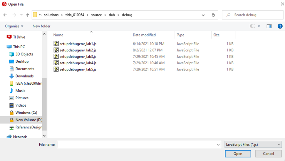 Figure 4-12 Select a Lab
- After running the script, the watch window is populated with the variables in Figure 4-13.
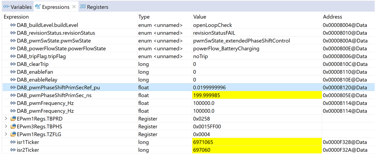 Figure 4-13 Watch Window
 - Enable Continuous refresh on the top right of the expression window.
- Enable PWM by writing “1” to the
DAB_clearTripvariable. (This variable resets to zero post writing and the normal.)
- Pass criteria for Lab1
Connect probes on PWM1A (Q1), PWM1B (Q2), PWM3A(Q5), and PWM3B (Q6).
1A and 1B are a complimentary pair, 3A is in sync with 1A with the specified phase shift, and the phase shift is controlled by the variable, DAB_pwmPhaseShiftPrimSecRef_pu.
Check the following:
- Frequency is 100 kHz
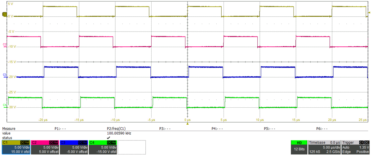 PWM1A (yellow), PWM1B (red), PWM3A (blue), PWM3B (green)Figure 4-14 100 kHz PWM
 - Now change the phase shift to 0.05 → 500 ns, to see more observable phase shift.
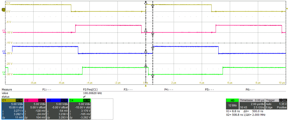 Figure 4-15 Phase Shift 500 ns
 - Verify on the
oscilloscope, that the phase shift matches the specified value. To
verify high-resolution operation select values which do not align with
the system-clock, which means are not divisible by 10 ns. In Figure 4-16 and
Figure 4-17, the
phase shift is measured using the oscilloscope to be approximately 500
ns for 500-ns setpoint and approximately 502 ns for a 502-ns setpoint, a
small jitter of approximately 1–2 ns can be the measurement error. CAUTION: Phase shift is not recommended to be operated beyond 0.45 pu.
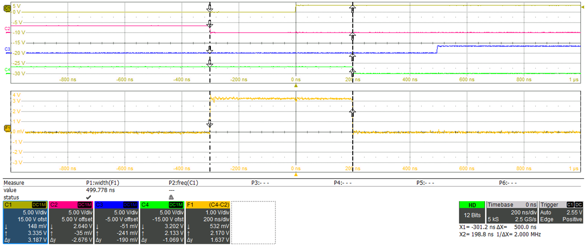 Phase shift is measured by using the math channel of the oscilloscope. The orange waveform is PWM3B – PWM1B. The width is equal to phase shift. The measured phase shift = 499.8 ns.Figure 4-16 High-Resolution Phase Shift 500 ns
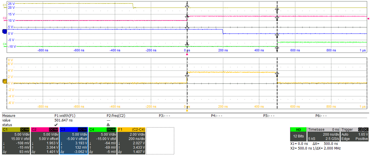 Phase shift is measured by using the math channel of the oscilloscope. The orange waveform is PWM3B – PWM1B. The width is equal to phase shift. The measured phase shift = 501.6 ns.Figure 4-17 High Resolution Phase Shift 502 ns
 - Change the PWM probes to PWM1A, PWM1B, PWM2A, and PWM2B.
- Verify PWM1A and 2B are in sync and in phase
- Verify PWM1B and 2A are in sync and in phase
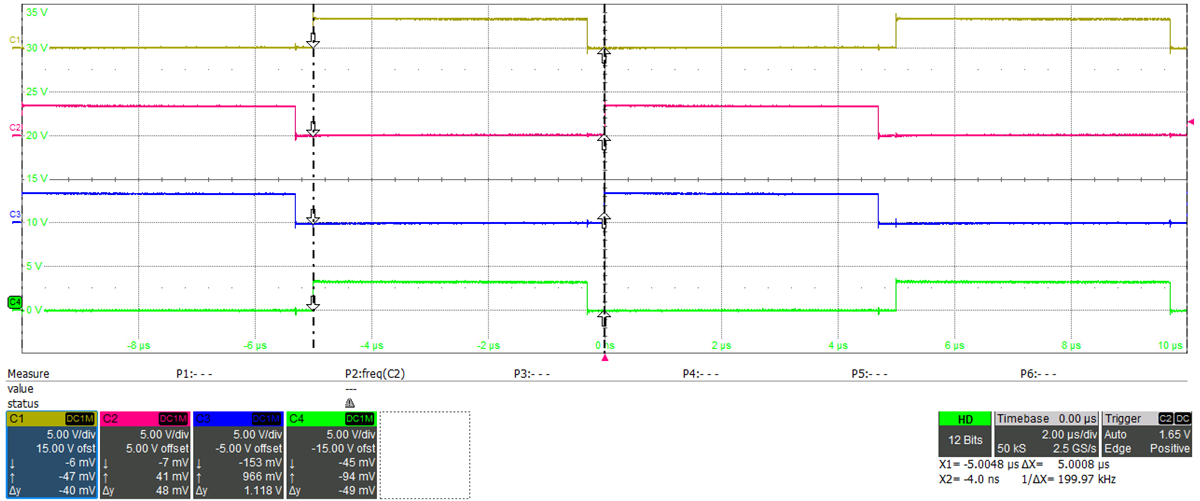 PWM1A (yellow), PWM1B (red), PWM2A (green), PWM2B (blue)Figure 4-18 PWM in Sync
 - Verify that they remain in sync and in phase as the phase shift for the secondary side PWM is changed.
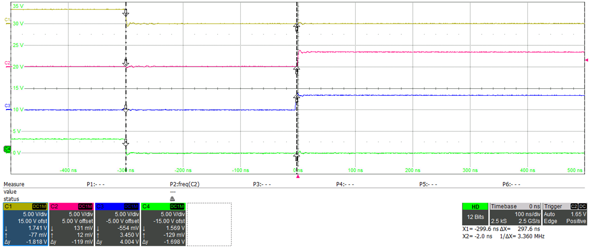 PWM1A (yellow), PWM1B (red), PWM2A (green), PWM2B (blue)Figure 4-19 PWM in Sync With Phase Shift
- Frequency is 100 kHz