TIDUES0E June 2019 – April 2024 TMS320F28P550SJ , TMS320F28P559SJ-Q1
- 1
- Description
- Resources
- Features
- Applications
- 6
- 1System Description
- 2System Overview
- 3Circuit Description
- 4Hardware, Software, Testing Requirements, and Test Results
- 5Design Files
- 6Related Documentation
- 7Terminology
- 8About the Author
- 9Revision History
2.3.2 Dual-Active Bridge – Switching Sequence
In a single-phase, dual-active bridge, primary and secondary bridges are controlled simultaneously. All switches operate at 50% duty ratio. The diagonal switches turn on and turn off together so that the output of each bridge is a square wave. The switching sequence of the converter is elaborated in detail in this section. For simplification the transformer is assumed with a windings ratio n = 1:1 and can be removed, for the description of the switching sequence.
The switching sequence is divided into four intervals based on the inductor current waveform and phase shift between the voltages at the primary and secondary of the transformer. The voltage and the current waveforms are depicted in Figure 2-10. During interval one, the inductor current waveform is both positive and negative, and hence, the current commutation follows the scheme shown in Figure 2-4 and Figure 2-5. During this interval, switches Q1 and Q4 in the primary and switches Q6 and Q7 in the secondary conduct current.
 Figure 2-4 Interval 1: Negative Inductor
Current
Figure 2-4 Interval 1: Negative Inductor
Current Figure 2-5 Interval 1: Positive Inductor
Current
Figure 2-5 Interval 1: Positive Inductor
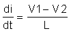
CurrentDuring this interval, the voltage across the primary, Vp, is equal to V1, and the voltage across the secondary, Vs, is equal to V2. The difference between these voltages appears across the leakage inductor, and the slope of the current during this interval can be approximated by Equation 2.
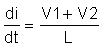
During interval two, the inductor current is positive. The voltage across the transformer primary is positive and is equal to V1, and the voltage across the secondary winding is positive and is equal to V2. Hence, the difference of these two voltages appears across the leakage inductor, and the slope of the rising current during this interval can be calculated by Equation 3.
During this interval, switches Q1 and Q4 remain turned on, but as the voltage across the secondary is now V2 with the inductor current positive, switches Q5 and Q8 turn on to conduct current. There is a small dead time period between the turn off of Q6 and Q7 and the turn on of Q5 and Q8. During this dead time, the phenomenon of zero voltage switching (ZVS) occurs, which is explained in detail in the following section. The commutation sequence for the second interval is shown in Figure 2-6.
 Figure 2-6 Interval 2
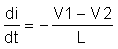
During interval three, the inductor current starts ramping down from the positive peak to a negative value as shown in Figure 2-10. In this interval, the voltage across the primary is –V1, and the voltage across the secondary is V2. The difference of these voltages, which is (-V1-V2), appears across the inductor. Hence, the current ramps down with a negative slope as shown in Equation 4.
During this interval, switches Q5 and Q8 continue to remain turned on, but as the voltage across the primary is now –V1, switches Q2 and Q3 turn on to conduct current. The conduction for both directions of inductor current IL > 0 and IL < 0 is shown in Figure 2-7 and Figure 2-8, respectively.
 Figure 2-7 Interval 3: Positive Inductor
Current
Figure 2-7 Interval 3: Positive Inductor
Current Figure 2-8 Interval 3: Negative Inductor
Current
Figure 2-8 Interval 3: Negative Inductor
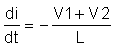
CurrentDuring interval four, the inductor current continues to be negative. During this interval, the voltage across the primary is –V1 and, and the voltage across the secondary is -V2. The difference in these voltages, which is (-V1+V2), appears across the inductor. Hence, the current ramps down with a negative slope as shown in Equation 5.
During this interval, switches Q2 and Q3 continue to remain turned on, but as the voltage across the secondary are now –V2, switches Q6 and Q7 turn on to conduct current as shown in Figure 2-9.
 Figure 2-9 Interval 4
Figure 2-10 shows the gating pulses of the switches on the primary and secondary side. The variable Ø represents the phase shift between the PWM pulses of the primary and secondary side. Vp and Vs represent the voltage on the primary and secondary winding of the transformer. IL represents the transformer current.
 Figure 2-10 Gate Signals, Transformer
Primary and Secondary Voltages, and Inductor Current
Figure 2-10 Gate Signals, Transformer
Primary and Secondary Voltages, and Inductor Current