TIDT292 June 2022
3.1 Switching
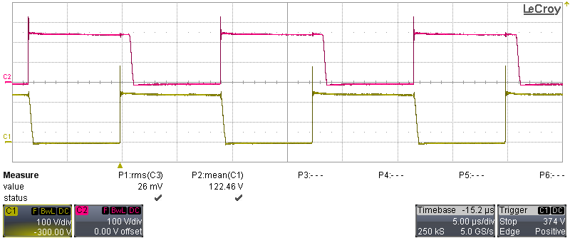
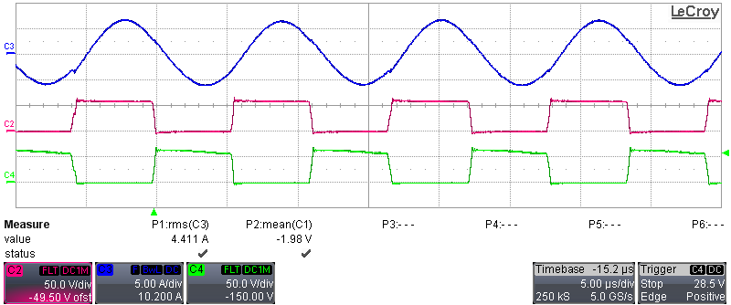
Switching waveforms on FETs of the PFC stage, as well primary-side FETs and sync FETs of the LLC stage, were taken by supplying the converter at 96 VAC and 115 VAC, F = 400 Hz, and full load.
 Figure 3-1 Drain-Source Voltages on Q1
and Q12 (C1: Q12-Vds, C2: Q1-Vds) at 96 VAC
 Figure 3-2 Drain-Source Voltages and
Resonant Current at 115 VAC (C4: Q7-Vds, C3: I(L7), C2: Q5-Vds
 Figure 3-3 Burst Mode Waveforms (C4:
Q7-Vds, C3: I(L7), C2: Q5-Vds) at 115 VAC and 200-mA Load