TIDT246 September 2021
4.1 Switching
The switching behavior of both converters is shown in the following figures. As in previous sections, the two converters were evaluated separately.
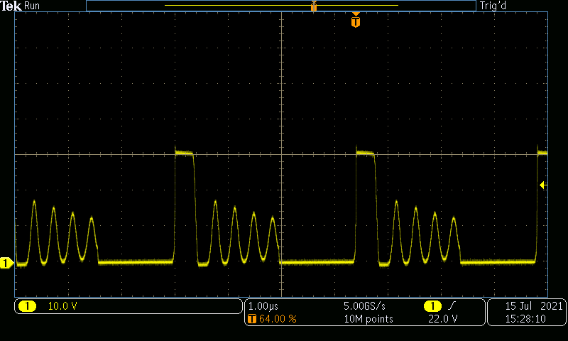 Figure 4-1 Boost Converter Switch Node, 6
VIN, Light Load
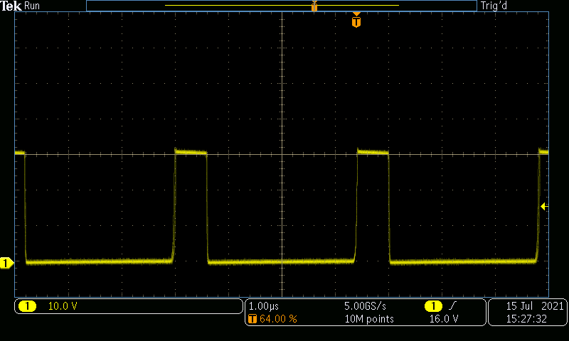 Figure 4-2 Boost Converter Switch Node, 6
VIN, Maximum Load
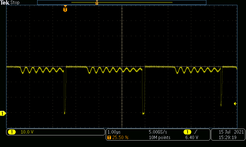 Figure 4-3 Boost Converter Switch Node, 28
VIN, Light Load
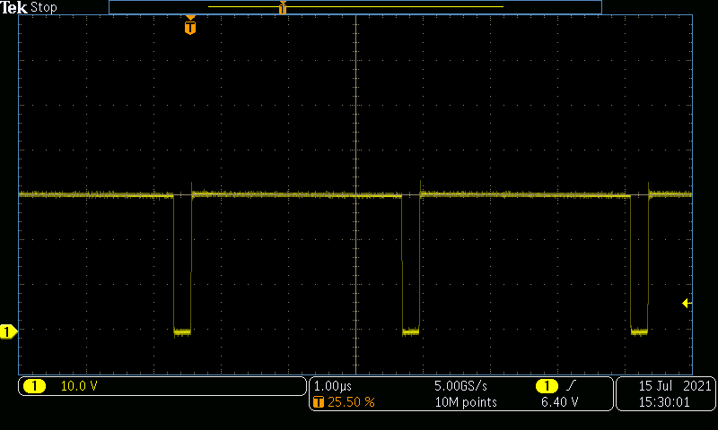 Figure 4-4 Boost Converter Switch Node, 28
VIN, Maximum Load
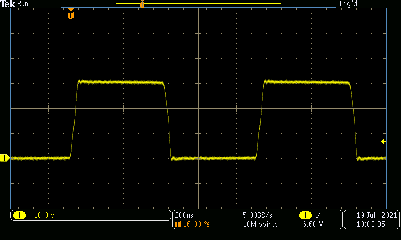 Figure 4-5 LLC Converter Primary Side Switch Node, 30
VIN, No Load
 Figure 4-6 LLC Converter Primary Side Switch Node, 30
VIN, 50% Load
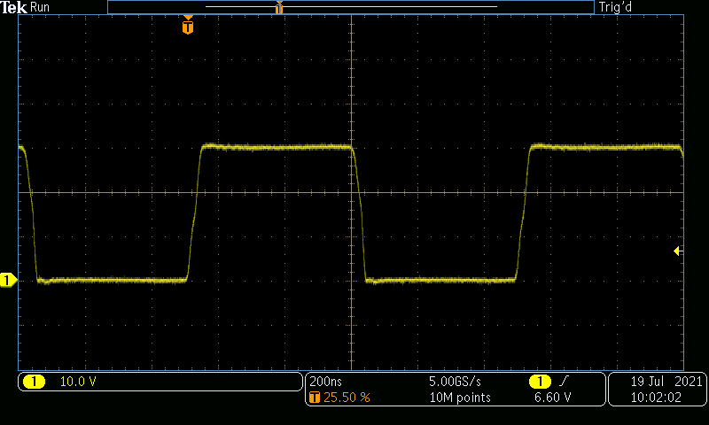 Figure 4-7 LLC Converter Primary Side Switch Node, 30
VIN, Max Load
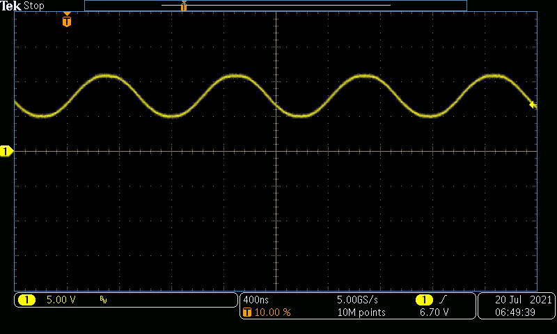 Figure 4-8 LLC Converter Secondary Side
Resonant Capacitor, 30 VIN, Max Load