TIDT246 September 2021
3.1 Efficiency and Power Dissipation Graphs
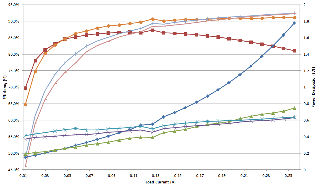
The efficiency of the boost converter and the open-loop LLC were measured separately. For the boost measurements the LLC was disabled by shorting the DIS/FLT pin of the UCC25800-Q1 (TP11) to GND and a resistive load was applied across the connector labeled VBOOST (J2). Efficiency curves were measured for inputs of 6 V, 12 V, 24 V, and 28 V.
 Figure 3-1 Boost Efficiency and Power Dissipation
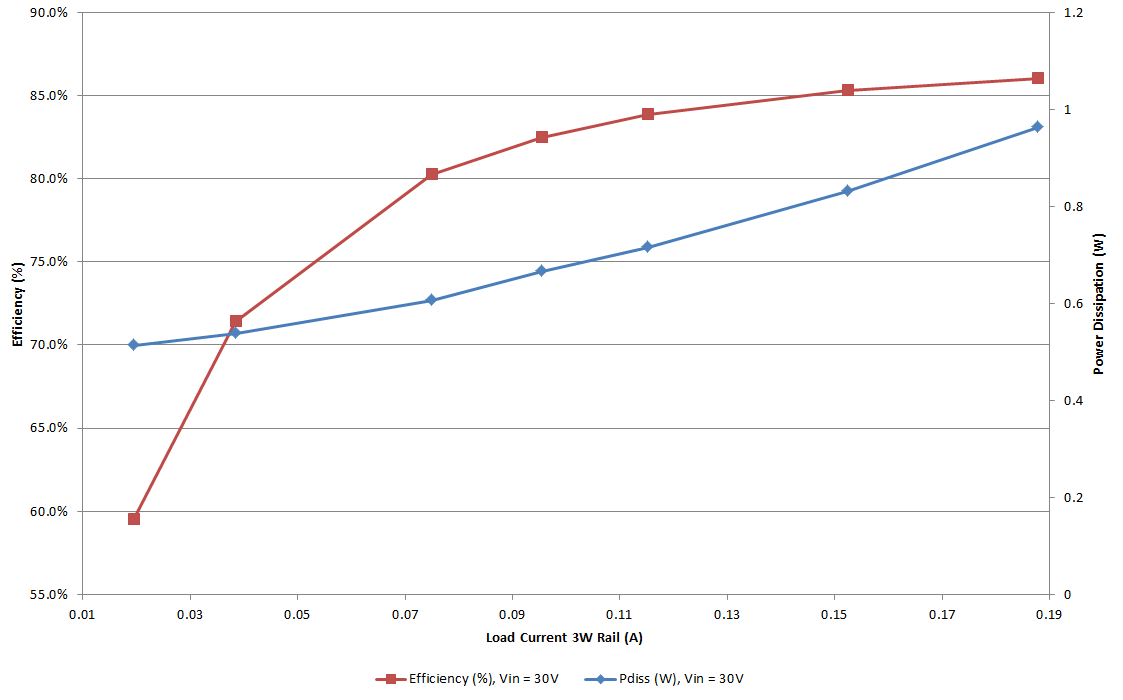
The LLC measurements were taken with a regulated 30 V applied at the connector labeled VBOOST (J2) and with the boost input (J1) disconnected.
 Figure 3-2 LLC Efficiency and Power Dissipation