TIDT236 March 2022 TPS7H1101A-SP
3.1 Switching
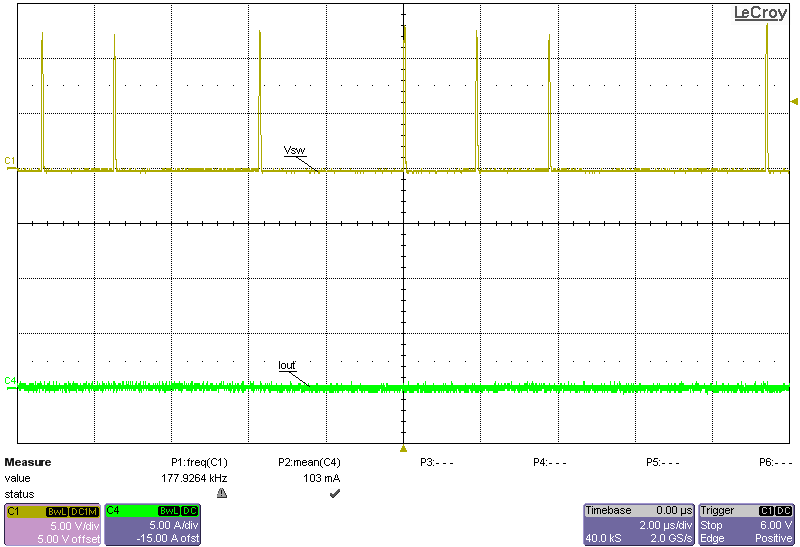
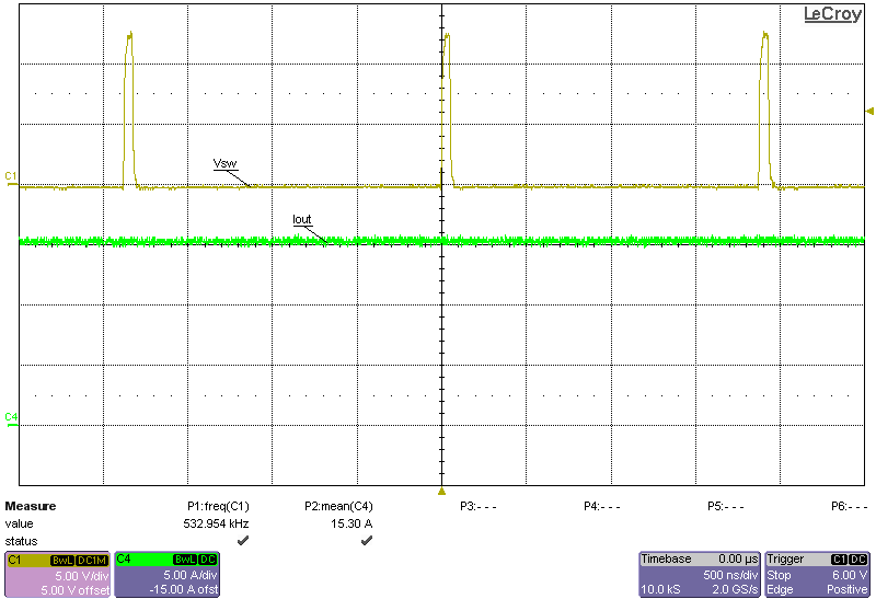
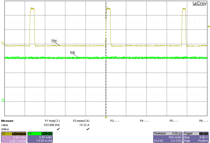
Figure 3-1 to Figure 3-4 show the switch node voltage of the converter at 12-V input and -0.2-V and -0.6-V output at no load and 15-A load conditions. Figure 3-1 illustrates that there are skipped pulses. This is due to the required ON-time pulses needing to be greater than the capable minimum ON-time of the regulator, which is 30 ns for the TPS543B20. This behavior tends to cease when the load is increased, which would require longer ON-time for regulation, due to the increase in duty cycle as power losses increase. The design should be evaluated for such behavior, especially for the boundary region of operation where the average switching frequency transitions from 500 kHz (with no pulse-skipping) to 250 kHz (that is, pulse-skipping; skipping every other pulse). The user needs to verify the operation and deem it acceptable under all their application scenarios, themselves.
 Figure 3-1 Switch Node Voltage, 12-V Input, –0.2-V
Output, No Load
 Figure 3-2 Switch Node Voltage, 12-V Input, –0.2-V
Output, 15-A Load
 Figure 3-3 Switch Node Voltage, 12-V Input, –0.6-V
Output, No Load
 Figure 3-4 Switch Node Voltage, 12-V Input, –0.6-V
Output, 15-A Load