TIDT200 September   2020


  1.   Description
  2. 1Test Prerequisites
    1. 1.1 Design Requirements
    2. 1.2 Required Equipment
    3. 1.3 Dimensions
  3. 2Testing and Results
    1. 2.1 Efficiency Graphs
    2. 2.2 Efficiency Data
    3. 2.3 Load Regulation
    4. 2.4 Thermal Images
    5. 2.5 EMI
  4. 3Waveforms
    1. 3.1 Switching
    2. 3.2 Output Voltage Ripple
    3. 3.3 Load Transients
    4. 3.4 Start-up Sequence
    5. 3.5 Undervoltage Protection

Switching

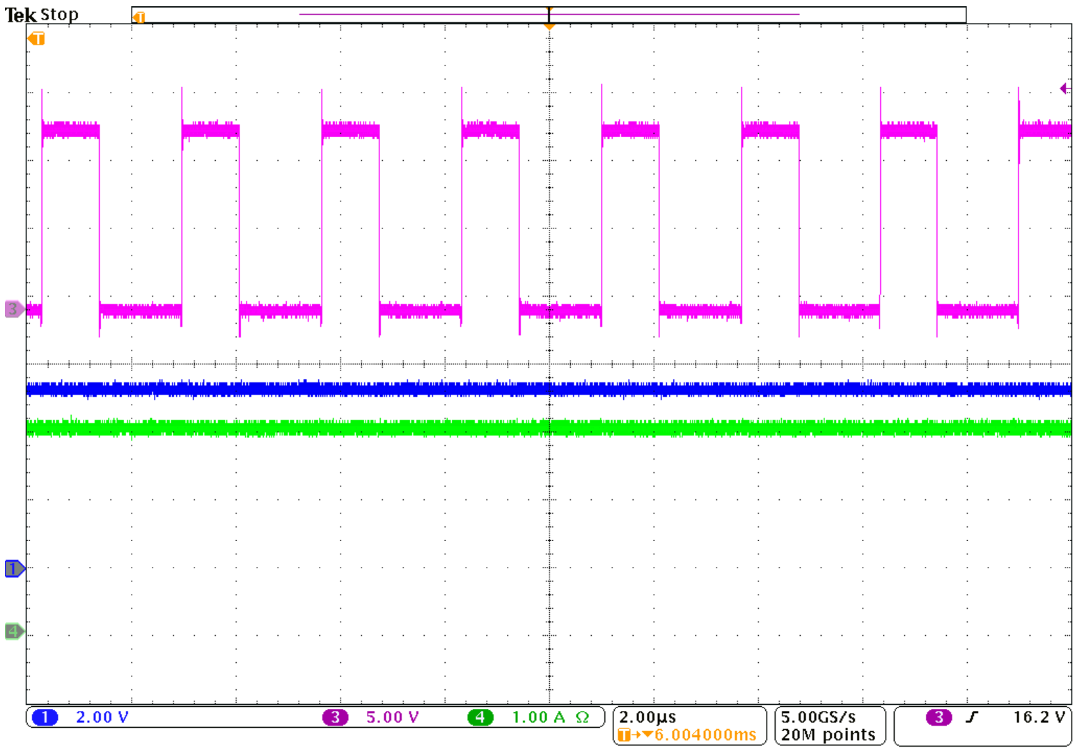
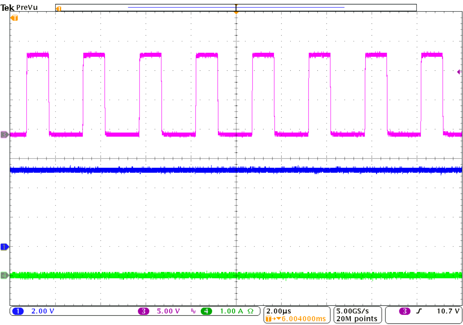
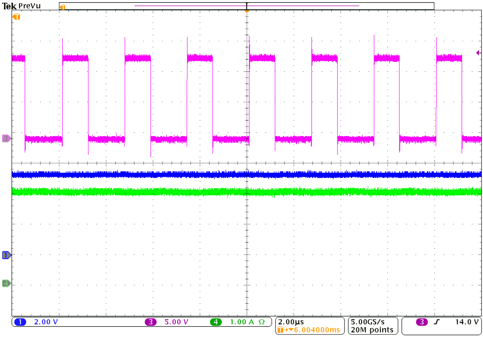
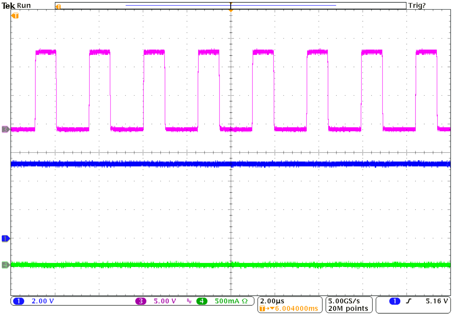
Switching behavior is shown in the following figures.
GUID-20200821-CA0I-CVDZ-GZJZ-GZP1N6PR4C1W-low.png
CH1: VPA_BUSCH3: VSWCH4: IPA_BUS
Figure 3-1 PA_BUS 13.5V input, 5.17V no-load
GUID-20200821-CA0I-VMZT-3WJ1-M5CXC6MKX6BZ-low.png
CH1: VPA_BUSCH3: VSWCH4: IPA_BUS
Figure 3-2 PA_BUS 13.5V input, 5.17V 3A load
GUID-20200821-CA0I-2RDW-NHS5-TBHG3ZRTTQM8-low.png
CH1: VPB_BUSCH3: VSWCH4: IPB_BUS
Figure 3-3 PB_BUS 13.5V input, 5.17V no-load
GUID-20200821-CA0I-Z5J0-8BXB-LXWXCNW3M7GR-low.png
CH1: VPB_BUSCH3: VSWCH4: IPB_BUS
Figure 3-4 PB_BUS 13.5V input, 5.17V 3A load