SWRA574B October 2017 – February 2020 AWR1243 , AWR2243
1 Cascaded AWR2243 System
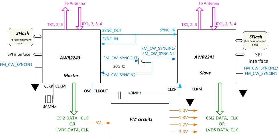
Multiple AWR2243 chips may be cascaded on PCB to improve target detection and resolution. In this section, two chip cascading and four chip cascading systems are illustrated as examples. The focus is on connection of various signals that the AWR2243 chips need to share among themselves. Of the multiple AWR2243 chips in the cascaded system, one is referred to as the Master and the others as Slaves. To make the entire cascaded system operate as a single radar system, the Master is designated to generate a common Local Oscillator (LO) signal (19 GHz to 20.25 GHz) shared across all the transmitters and receivers in the entire cascade system. The master also controls the radar chirp/frame timing for all the chips by generating a digital Sync signal and sharing this synchronization signal with the slaves. The master also uses a 40 MHz crystal and generates a 40 MHz oscillator clock (OSC_CLKOUT) and shares it with the slaves (as CLKP), thereby eliminating the need for additional crystals on the slaves and ensuring that the entire system operates from a single clock source.
The master is capable of supplying the shared LO on two different output pins through two different delay matched amplifiers. This can be used in a four chip cascade system to supply the LO signal to the master and three slaves using only passive splitters. This eliminates the need for additional, costly, active components on the PCB. The OSC_CLKOUT pin is used by the master to share the the 40 MHz clock source with the slave devices in the system. In the case of a 2-device system, this can be done with just a passive trace between devices. In the case of more than 2-devices, it is recommended to use a clock fan-out buffer to manage loading and signal integrity issues. Similarly, the DIG_SYNC is conveyed from the master to the slaves and back to itself through delay matched buffers on board.
Other than these connections which are illustrated in the below diagrams and further elaborated in later sections, the cascaded system also has Power Management ICs (PMIC) (each PMIC can handle up to two AWR2243 chips), an optional QSPI Flash (needed for initial software development purpose only) and the mmWave antennas connected to each AWR2243 chip.
 Figure 1. A Two Chip Cascade System
  Figure 2. A Four Chip Cascade System