SSZT624 september 2018 LM5109B , UCC27710 , UCC27712 , UCC27734 , UCC27734-Q1 , UCC27735 , UCC27735-Q1
Have you ever been watching your favorite show and noticed a blur or partial screen freeze? I think it was caused by an incorrect timing of the refresh.
For proper operation in a half-bridge power train, such as DC drives, it is important that the timing to the high and low-side power devices is correct. In the case of watching TV, a timing glitch is just annoying. But in a half-bridge power train, timing glitches in the high-side and low-side power devices can interrupt the intended operation, or even cause a failure in half-bridge power metal oxide semiconductor field effect transistors (MOSFETs).
There are important design details to consider in order to achieve higher system robustness when selecting a gate driver for your DC drives. In part 1 of this series (How to achieve higher system robustness in DC drives part 1: negative voltage) German Aguirre discussed negative voltage spikes on the switch-node HS pin, and in part 2 of this series (How to achieve higher system robustness in dc drives part 2 interlock and deadtime) I discussed output interlock and deadtime. In this installment, I’ll discuss the minimum input pulse rejection feature.
Minimum input pulse rejection prevents the outputs (LO and HO) from responding to a pulse width less than the allowable minimum input pulse requirement, thus preventing the driver outputs from responding to narrow spikes or ringing, generating an unexpected driver output pulse, and having the MOSFETs from turn on at the incorrect time.
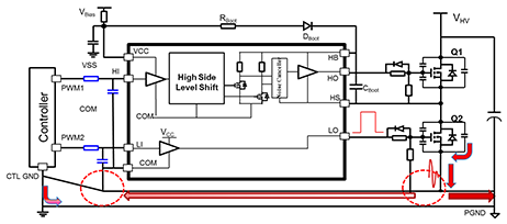
Voltage spikes and ringing on the driver input signals caused by current spikes flowing in the control ground paths are a common problem in motor control. Figure 1 shows the board layout trace ground paths that exist in many designs. In many cases, it is not possible to eliminate the potential for current flowing in the control ground, so you will need a robust gate driver to handle the transients that they cause.
The red arrows in Figure 1 show low-side turn on during hard switching operation: the falling VDS voltage generates a current spike upon discharge of the switch node capacitance. This high dI/dt current spike will flow through the ground path and return to the input capacitance. As the driver ground (COM) typically connects close to the MOSFET source, and the controller in many cases connects to the driver ground, a parallel current path exists from the MOSFET source, (COM) and controller. This can result in a significant current spike flowing into the control-referenced ground.
 Figure 1 Driver Input Voltage
Spikes/ringing from Ground Current
Figure 1 Driver Input Voltage
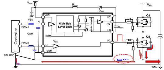
Spikes/ringing from Ground CurrentAdding a high-frequency impedance such as inductance or resistance to the path between the MOSFET source and the driver/controller ground reference can reduce the current flowing into the controller, as shown in Figure 2.
 Figure 2 Impedance in Ground Path to
Reduce Control Ground Current
Figure 2 Impedance in Ground Path to
Reduce Control Ground CurrentIt’s important that gate drivers have features that can tolerate voltage spikes in order to ensure reliable operation and improve robustness in your designs. The UCC27710 driver’s minimum input pulse feature prevents the LO and HO outputs from responding to narrow spikes and ringing. This driver rejects low to high pulses and high to low pulses less than 40ns as shown in Figure 3, and thus prevents driver input noise from causing the power MOSFETs to unexpectedly turn on or off.
 Figure 3 LO and HO Response with
Positive and Negative Narrow Pulses
Figure 3 LO and HO Response with
Positive and Negative Narrow PulsesLet’s look at ways to reduce ground current voltage spikes on the driver inputs. You can add resistance or inductance to reduce current in the control ground. This resistance or inductance creates a high-frequency impedance.
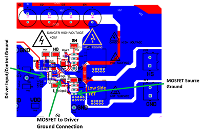
Figure 4 shows an example half-bridge driver and power-train layout. You can see that the low-side MOSFET connects to a large ground path and the driver input connects to a large ground path. But the large ground planes are not continuous from power to driver input or control.
 Figure 4 MOSFET to Control Ground
Connection to Limit Current Spike
Figure 4 MOSFET to Control Ground
Connection to Limit Current SpikeIf the MOSFET source to control ground has a higher inductance than the power and control planes, the current spike will be reduced in this path relative to the large power plane. The narrower trace connection shown in Figure 4 will result in a higher inductance path.
In part 2 of this series (How to achieve higher system robustness in dc drives part 2 interlock and deadtime) I provided other layout tips on how to reduce noise on the driver inputs.
TI gate drivers with minimum input pulse rejection provide higher system robustness when designing motor drives.
Additional Resources
- These designs from the TI Designs reference design library showcase gate drivers in DC drive and appliance subsystems:
- Watch these training videos:
- The UCC27712 and LM5109B TI gate drivers are candidates for DC drive applications: