SNVAA30 December 2021 LM5170-Q1
2.3 Outer Voltage Loop Design
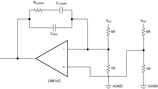
To implement outer voltage loop, an external Op-Amp (Texas Instruments LM6142) is used. The Op-Amp keeps constant ratio between VHV and VLV. The non-inverting input of the Op-Amp is connected to the 9R:1R resistor divider on the VHV rail, and the inverting input is fed by the 4R:1R resistor divider on the VLV rail. Therefore, the Op-Amp’s non-inverting input voltage is at 1R/10R × VHV, and the inverting input at 1R/5R × VLV. In the closed loop operation, VHV = 2 × VLV, namely the two battery voltages are balanced.
 Figure 2-4 Outer Voltage Loop Control in
LM5170-Q1
Figure 2-4 Outer Voltage Loop Control in
LM5170-Q1A Type II compensation network is used to stabilize the outer voltage loop. Figure 2-4 shows configuration of type II compensation network consisting of RCOMP2, CCOMP2 , and CHF2. The introduced poles and zero of compensation network are determined by
where RL is load equivalent resistance and Co is output capacitance.
To tailor the total voltage loop gain to cross over at FCO_VOL, select components of the compensation network according to the following guidelines, then fine tune the network for optimal loop performance.
- The FCO_VOL is set to 1/5 or 1/10 of FCO_CUR
- The total outer voltage loop gain is set to unity at FCO_VOL
- The zero FZ_COMP is placed at the power stage power FP_PLANT
- The pole FP_COMP is placed at approximately one or two decades higher than FZ_COMP, but lower than FSW
Select RCOMP2 = 270 kΩ, CCOMP2 = 2.7 nF, and CHF2 = 13 pF which can meet the following equations.
Figure 2-5 shows bode plot of outer voltage loop. Phase in mid-frequency range is boosted by type II compensation network. In this example, the crossover frequency is at about 4 kHz, and the phase margin is approximately 75 degree, which is greatly higher than the needed minimal 45 degree of a stable system. FP_COMP is placed at 45.34 kHz which is lower than switching frequency (99.5 kHz) to minimize output ripple caused by MOSFET switching.