SNVAA29 October 2021 TPS542A50 , TPS543320 , TPS543B20 , TPS543C20A , TPS546A24A , TPS546B24A , TPS546D24A , TPS548A28 , TPS548B28 , TPS54J061
3 Voltage Regulation Accuracy
As the semiconductor process technology advances, processors require tighter voltage accuracy and lower operating voltages. The processor data sheet specifies the voltage tolerance as either a percentage or as a value in mV, which includes DC, AC and ripple variations over the entire operating temperature range. Designers also consider the tolerance of the resistor divider used by the DC/DC converter, the routing and trace losses of the circuit board, and the variations of the application, like the input voltage variations, temperature swings, and fast changes in the load.
Check the feedback voltage accuracy of the DC/DC converter in the data sheet rather than the front page. Table 3-1 shows the regulated feedback voltage, or the internal voltage reference specification of the TPS548A29, which is a 2.7 V to 16 V, 15-A converter, and shows that the reference accuracy is ±6 mV or ±1% over the full temperature range. The total output voltage accuracy is improved by choosing tighter tolerance resistors. If more headroom is needed, designers can choose 0.1% or 0.5% resistors, even though they may cost a little bit more. The additional headroom allows a total ±3% or ±5% output voltage variation to be met with less bulk and bypass capacitance. (1)
| Parameter | Test Condition | Minimum | TYP | Maximum | Unit |
|---|---|---|---|---|---|
| Internal Voltage Reference | TJ = –40°C to 125°C, VCC = 3 V | 594 | 600 | 606 | mV |
| TJ = 0°C to 85°C, VCC = 3 V | 597 | 600 | 603 | mV |
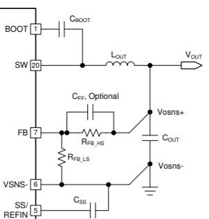
Layout constraints, connectors, and board density requirements affect the total output voltage accuracy. A remote sense feature of a DC/DC converter compensates for voltage drops from long trace lines to accommodate processors needing high accuracy output voltage. This feature is especially useful when routing higher currents since the voltage drop can be a large portion of the overall DC error.
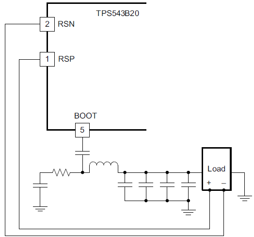
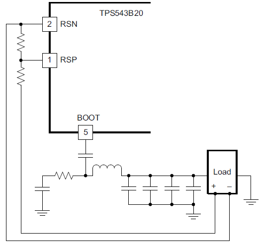
Figure 3-1 shows the TPS543B20 using the remote sense feature with voltage feedback resistors used to program the output voltage. Figure 3-2 shows the TPS543B20 using the remote sense feature without voltage feedback resistors when the VSEL pin selects the reference voltage. The RSP and RSN pins are extremely high-impedance input terminals of a true differential remote sense amplifier.
 Figure 3-1 TPS543B20 Remote Sense Without
Feedback Resistors
 Figure 3-2 TPS543B20 Remote Sense With
Feedback Resistors
 Figure 3-3 TPS548A29 Differential Remote
Sense Implementation