SNOU172 December 2020
3.1 LM74500Q1EVM Performance Capture
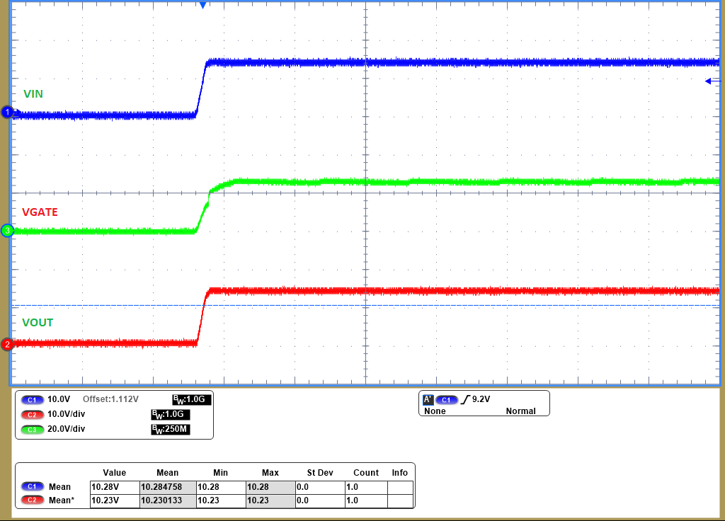
A startup pulse from 0 V to 12 V is applied at the input of the LM74500Q1EVM. Figure 3-1 shows the input voltage (CH1) rises from 0 V to 12 V and the gate voltage (CH3) comes up after input voltage crosses device PoR threshold . The gate of external N-FET is fully enhanced and FET is turned on. Output voltage (CH2) rises smoothly from 0 V to 12 V.
 Figure 3-1 LM74500Q1EVM Startup
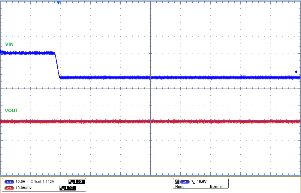
A –12 V source is connected to the VIN input of the LM74500Q1EVM. Figure 3-2 shows that the output voltage remains at a constant 0 V in this situation. This test simulates the event of connecting a 12-V battery in the reverse direction; therefore, protecting the load from negative input voltages.
 Figure 3-2 Startup Reverse Polarity (–12
V)