SNOU172 December 2020
2.1 I/O Connector Description
-
VIN
J1: Power input connector to the positive rail of the input power
supply
-
GND1
J3: Ground connection for the power supply
-
VOUT
J2: Power output connector to the positive side of the load
-
GND2
J4: Ground connection for the load
-
Test Points
VIN, VOUT, GND1, and GND2 are test points
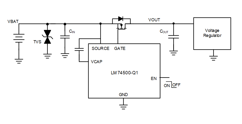
 Figure 2-1 LM745000Q1EVM Typical Application Circuit