SNOAA75A June 2021 – April 2022 LMP7704-SP
Design Steps
Photodiode Sensor Parameters
This circuit considers Hamamatsu’s S1336-5BK Si photodiode, which is targeted for UV to NIR precision photometry applications. Some of the key specifications are:
- Diode Capacitance (CPD) = 65 pF
- Shunt Resistance (RPD) = 1 GΩ
- Maximum Reverse Current (IPD(max)) = 20 μA
Transimpedance Gain Calculation
First, to determine the maximum transimpedance gain, consider two factors: the maximum reverse current, IPD(max), and the desired output voltage range, VOUT(max) and VOUT(min). The minimum voltage range is determined to be 0.2 V so that the amplifier does not saturate to V– or GND in this case. The value of the feedback resistor (RF), which sets the transimpedance amplifier (TIA) gain can be calculated by dividing the maximum output by the maximum reverse current:
Feedback Capacitor Calculation
The feedback capacitor, in combination with the feedback resistor, forms a pole (fP) in the frequency response of the amplifier:
Above this pole frequency, the amplification of the circuit declines. The maximum feedback capacitor value can be determined from the feedback resistor value and the desired bandwidth:
Keeping the feedback capacitor at or below the calculated value, ensures that thecircuit meets the stated bandwidth requirements. In this case, 10 pF is chosen as the closest standard capacitor below the value calculated for CF.
Bias Network Calculations
The photodiode acts as a reverse biased diode at DC, so the gain from the non-inverting terminal of the op amp is 1. Therefore, when the photodiode current is 0 A, VOUT = VBias. Consider the case where VBias is 0 V and an amplifier has a maximum output voltage swing (VOUT) of 200 mV. If the photodiode current is 0 A, the amplifier with a noise gain of 1 attempts to produce a 0-V output, resulting in the amplifier saturating and its bandwidth compromised due to the saturation recovery time. It is best to account for the VOUT requirement of the amplifier by adding a bias voltage that defaults the TIA output above the maximum VOUT from the negative rail. The bias at the non-inverting input is given by the equation:
For many rail-to-rail input/output (RRIO) op amps, the typical output swing limitations range from 30 to 60 mV depending on operating conditions, and in some instances can be as high as 200 mV. A bias voltage (VBias) of 200 mV is used to account for the worst-case scenario.
Selecting a value for RB2 of 10 kΩ, calculate RB1 to be:
Capacitor CB is placed in parallel with resistor RB2 to reduce the noise contribution of the resistor divider and prevent power supply noise from affecting the amplifier output. Selecting a value of 1 μF for CB produces a corner frequency (fc) of:
The calculated corner frequency should be low enough to prevent power supply noise from passing to the output.
Amplifier Gain Bandwidth Calculation
Having calculated the maximum feedback capacitor value allowable to meet the bandwidth design requirement, it is necessary to calculate the necessary op amp gain bandwidth for the circuit to be stable.
The following figure shows a version of the circuit which has been redrawn to include the photodiode junction capacitance (CPD) and the differential (CD) and common-mode (CCM-, CCM+) input capacitances of the amplifier. The bias voltage applied to the non-inverting input is considered an AC ground.
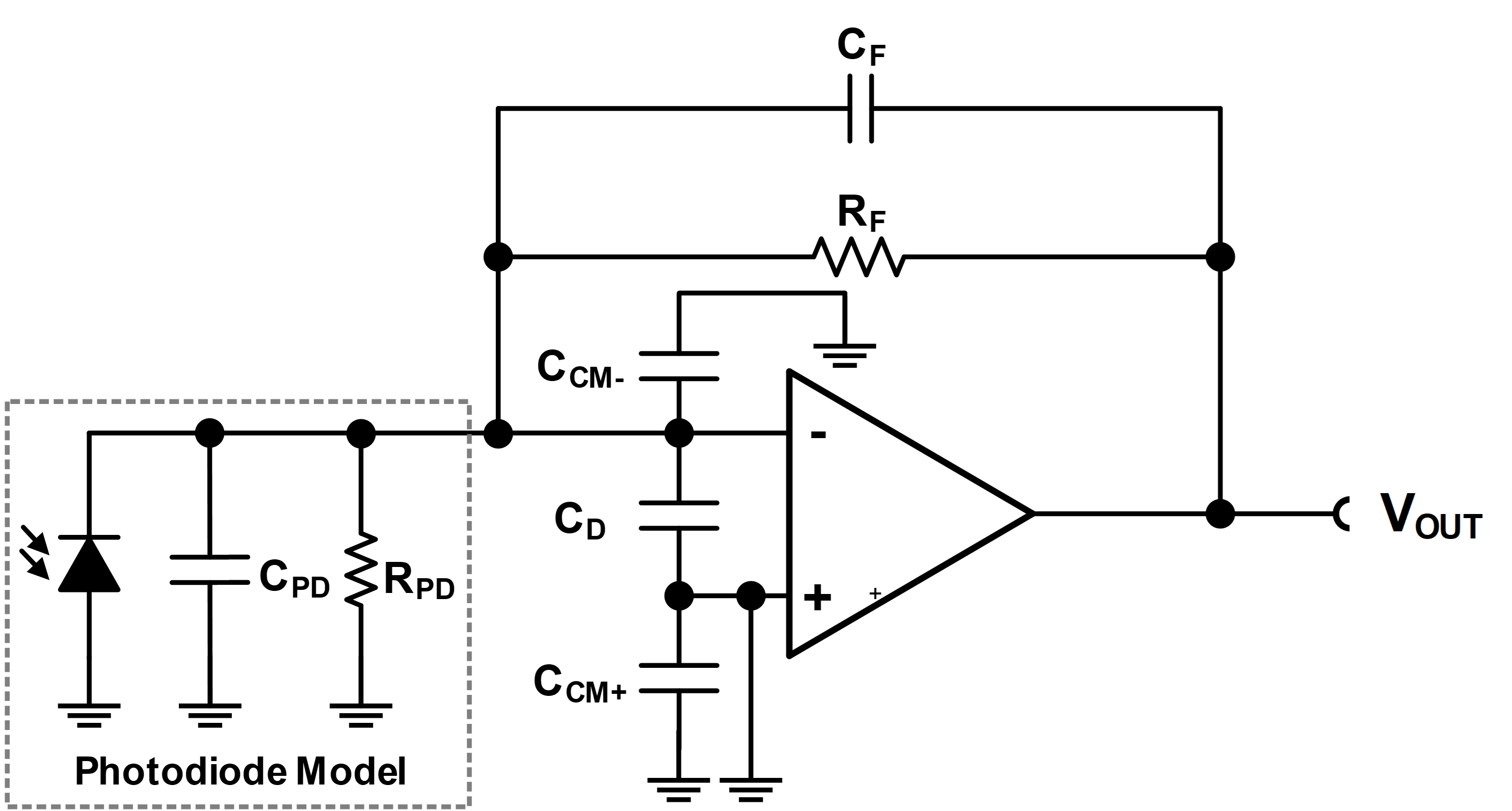
From this illustration it is apparent that CPD, CD, and CCM- are in parallel and the capacitance at the inverting input is described by the following equation:
To calculate the unity gain bandwidth (UGBW) requirement for this design, CIN must first be determined. CD and CCM– are not known at this time since a specific op amp has not been selected, but 10 pF can be used as a reasonable guess for the sum of these values. The exact value can be substituted later to confirm the appropriateness of an op amp.
Now, the values for CF, RF, and CIN can be inserted into the following equation to find the target op amp gain bandwidth (GBW):
Op Amp Selection
The basic requirements for the op amp used in this application are outlined in the following table:
| Specification | Design Goal |
|---|---|
| Total Ionizing Dose (TID) (krad(Si)) |
100 |
| SEL Immunity (MeV·cm2/mg) | 85 |
| VCC Range (V) |
2.7–5.5 |
|
VCC Abs Max (V) |
> 6.3 |
|
Input Bias Current (pA) |
< 1000 |
|
Typ. Iq per Channel (mA) |
< 2.0 |
|
Input Voltage Range (Typ) |
(V–) + 200 mV |
| Output Voltage Range (Typ) | (V–) + 200 mV, (V+) – 200 mV |
|
GBW |
> 1.176 MHz |
The requirements for supply voltage and current were given in the design requirements. The input and output voltage range requirements are selected to ensure linear operation over the desired signal amplitudes. Finally, the gain bandwidth requirement was calculated in the Amplifier Gain Bandwidth Calculation section.
In addition to these basic requirements, the op amp should contribute negligible errors from voltage offset, input bias current, and voltage or current noise. Op amps with JFET or CMOS inputs are the most commonly-selected type because these op amps typically have much lower bias current than those with BJT input devices. This results in reduced DC error voltages and lower noise due to reduced input current noise. A complete noise analysis of this amplifier is beyond the scope of this document, see reference6 for more information on noise in photodiode amplifiers. Zero-drift amplifiers or amplifiers with chopper inputs such as LMP2012QML-SP should be avoided due to the nature of the chopper input stage, the input bias current is not constant. The input MOSFET chopping stage creates dynamic transient currents on the inputs due to charge injection, which differ from the actual static bias current and could cause transients at the circuit output if the switching frequency is below the cutoff frequency.
The LMP7704-SP was selected for this design because of its excellent combination of low bias current (as an op amp with CMOS inputs), offset voltage, power consumption, radiation performance and wider supply range, which could allow for re-use in other applications in the system, as well as use without a bias voltage in systems that have bipolar voltage rails available. Relevant LMP7704-SP specifications are given in the following table:
| Specification | Target | LMP7704-SP |
|---|---|---|
| TID (krad(Si)) |
100 |
100 |
| SEL Immunity (MeV·cm2/mg) | 85 | 85 |
| VCC Range (V) |
2.7–5.5 |
2.7–12 |
|
VCC Abs Max (V) |
> 6.3 |
13.2 |
| VOS (Max. at 25°C) (μV) | – |
200 |
|
Input Bias Current (pA) |
< 1000 |
0.2 |
|
Typ. Iq per Channel (mA) |
< 2.00 |
0.73 |
|
Input Voltage Range (Typ) |
(VEE) + 200mV |
(VEE) – 200 mV |
| Output Voltage Range (Typ) | (VEE) + 200mV, (VCC) – 200mV | (VEE) + 50mV, (VCC) – 60mV |
|
GBW (MHz) |
> 1.176 |
2.500 |
| Slew Rate (V/µs) | – | 1 |
The LMP7704-SP meets or exceeds all required specifications for the design. However, the parallel combination of the differential and common-mode input capacitances (CD + CCM–) is 25 pF, which is higher than the estimated value used to calculate the required gain bandwidth product, so the gain bandwidth requirement previously calculated should be re-calculated to verify that the GBW of the LMP7704-SP is sufficient.
LMP7704-SP has 2.5 MHz of gain bandwidth (GBW), which provides more than enough adequate margin to achieve a stable design. It should also be noted that the slew rate (SR) of the op amp might be a limitation to the full power bandwidth of the circuit, the full power bandwidth is the highest frequency sinusoid that can be reproduced at the full output swing of the amplifier. The full power bandwidth (fFP) can be calculated using the equation:
"SR" is the slew rate of the op amp in Volts per Second, and "A" is the amplitude of the sinusoid. The full output swing of this amplifier is from 0.2 V to 2.5 V, or a swing of 2.3 V. Therefore the amplitude of the sinusoid is 2.3 V / 2 = 1.15 V. The resulting full power bandwidth is:
The resulting full power bandwidth is above the TIA bandwidth, so SR limitations should not be a significant contributing factor to distortion for full-scale signals.