SNOAA75A June 2021 – April 2022 LMP7704-SP
Design Simulations
Simulation
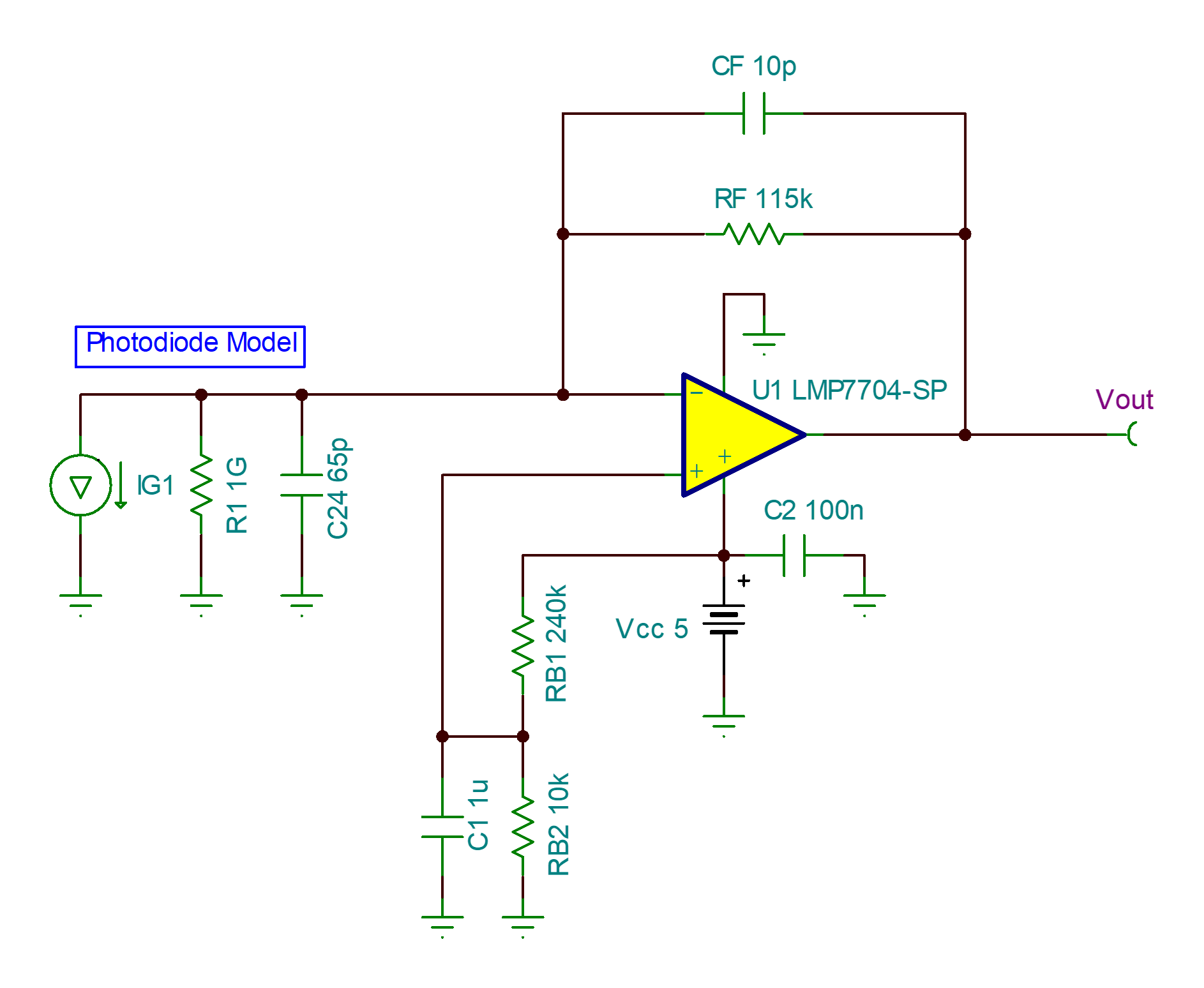
The following figure shows the TINA-TI™ simulation schematic of the photodiode amplifier. The current source IG1 and the capacitor C24 serve to form a simple model that represents the reverse current, IPD, of the photodiode and junction capacitance CPD, respectively.
DC Transfer Function
A DC transfer characteristic analysis is used to verify the gain and output voltages of the circuit. The output current of IG1 is swept from 0 to 20 μA and the output voltage is plotted.
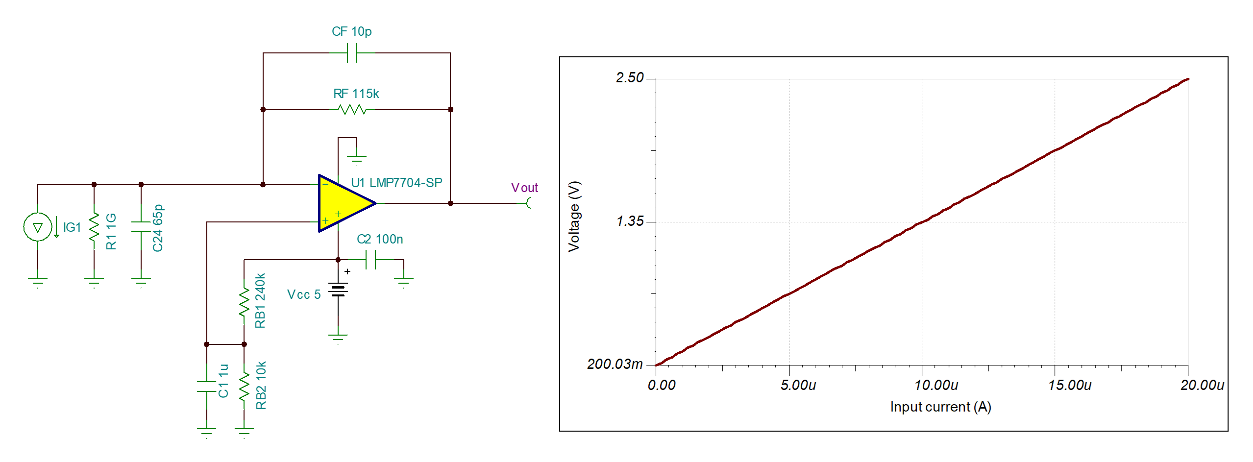
For zero input current, the simulated output voltage is 200.032 mV, and at 20-μA input current, the simulated output voltage is 2.500 V and the gain is 115 kV/A.
AC Transfer Function
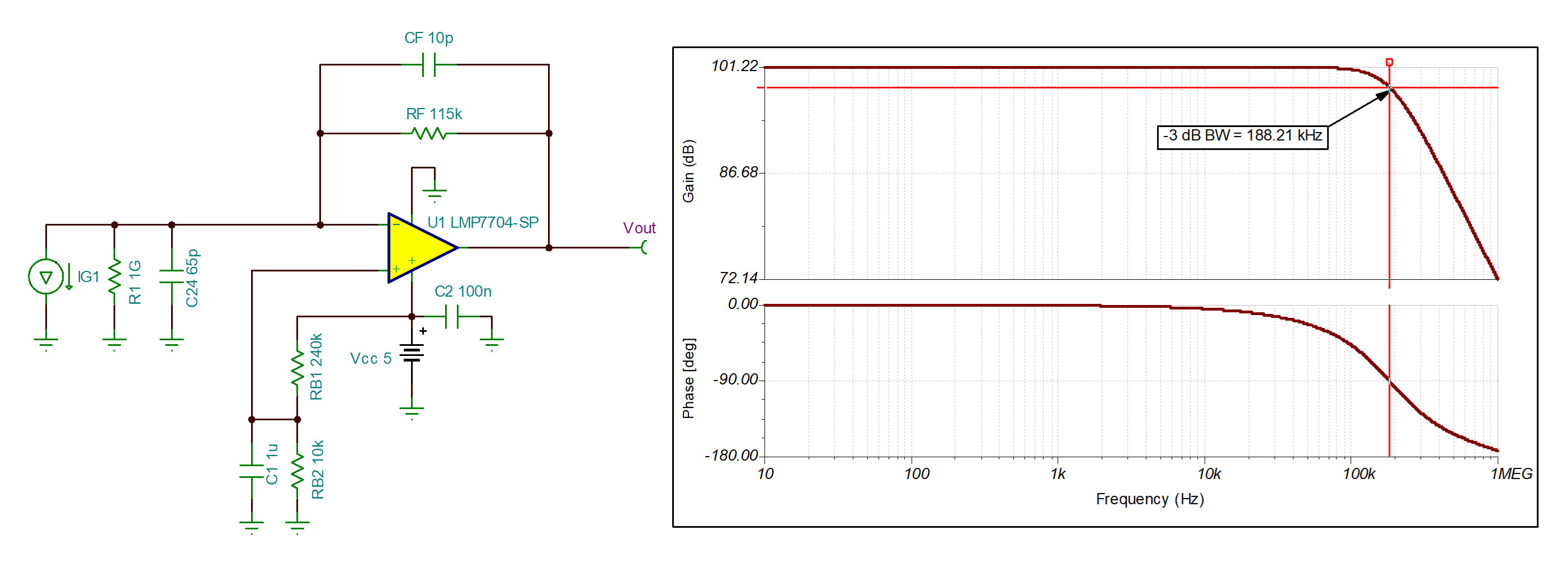
The AC transfer function was measured using an AC transfer characteristic analysis in TINA-TI™. The simulated –3-dB point was 188.21 kHz.
Stability Analysis
For simulation of the loop stability, the feedback path of the amplifier is broken at the output using a large inductor (Ltest). This inductor allows the circuit to converge to the proper DC bias point but acts as an open circuit in an AC transfer characteristic simulation. Voltage source V_AC is AC coupled into the feedback loop by capacitor (Ctest) and the loop gain is measured by voltage probe Vout.
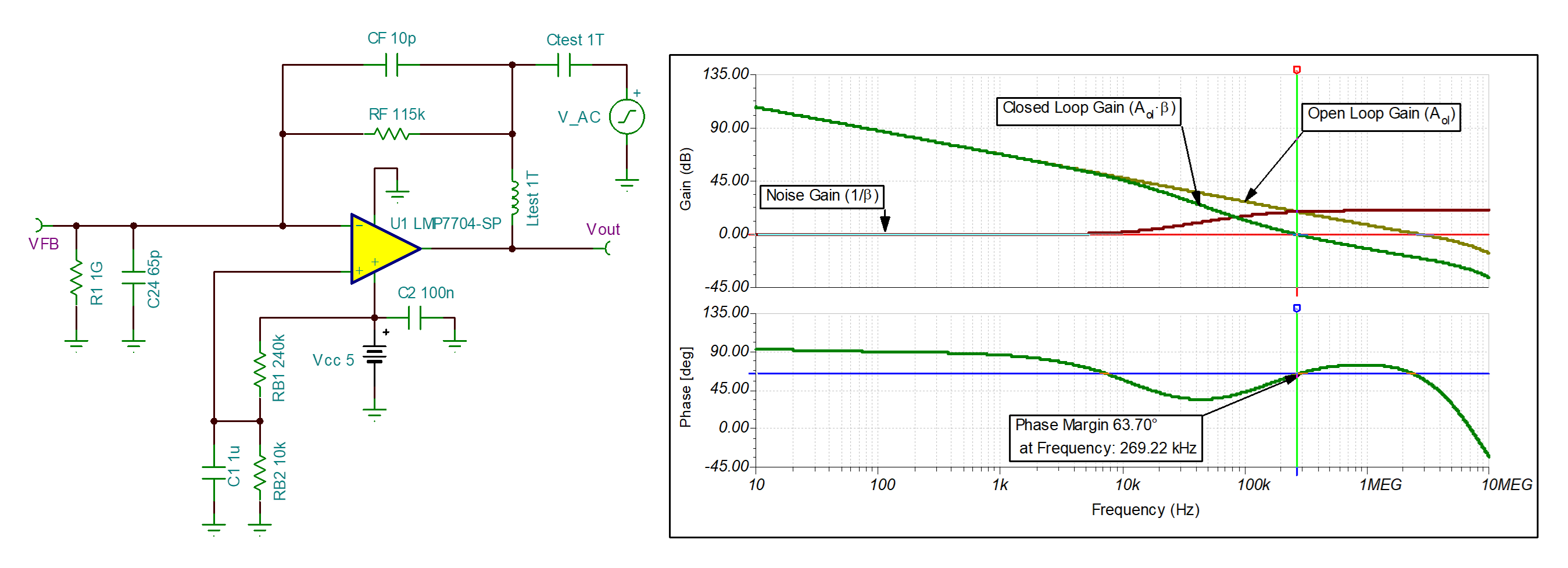
The loop gain plot shows the loop closure point (loop gain is 0 dB) at 269.22 kHz with 63.70 degrees of phase margin.