SNLU317A september 2022 – may 2023 DP83867E
1.1 Overview
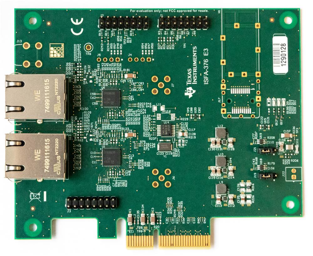
 Figure 1-1 DP83867 Dual-Port TSN PCIe
Application Interface Card (Top View)
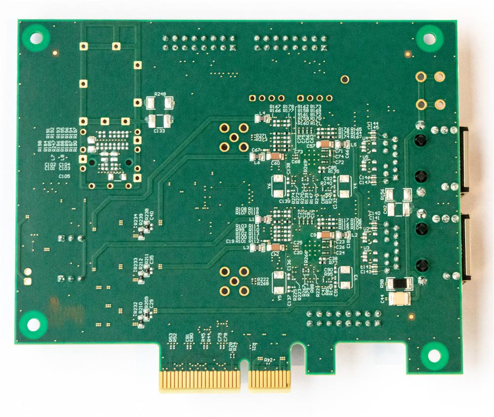
 Figure 1-2 DP83867 Dual-Port TSN PCIe
Application Interface Card (Bottom View)
Figure 1-2 DP83867 Dual-Port TSN PCIe
Application Interface Card (Bottom View)The DP83867 Dual-Port TSN PCIe Application Interface Card plugs into the Intel Tiger Lake or Alder Lake reference design through the PCIe interface connector. This is an easy way to evaluate the functionality of the DP83867 Ethernet PHY with the Intel CPU reference design.
Note that the PCIe interface connector is used only as a form factor and uses proprietary interface signal assignment as given by the Intel reference design. The PCIe form factor carries the SGMII signaling for two Ethernet ports, MDIO/MDC, power supply and control signals.
The AIC supports MDIO access via dedicated a SMI interface over the PCIe interface. The two DP83867 PHYs use different MDIO addresses to be addressed via the common interface.
For easy testing and development purpose, the AIC card supports several pin headers for signal probing.
The AIC uses the two RJ45 jack LEDs to show PHY link and speed indication with one LED, and PHY data transfer activity with the second LED.