SNAK010 April 2022 ADC128S102-SEP
2.3.1 Biased
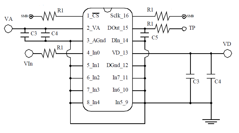
Figure 2-1 shows the bias conditions for each pin during irradiation. Table 2-1 describes the pin signal connections.
 Figure 2-1 ADC128S102PW-SEP Biased Diagram
Table 2-1 Pin Signal Connections
|
Symbol |
Limits |
|
|---|---|---|
|
MIN |
MAX |
|
|
VA and VD |
5.0 V |
5.5 V |
|
Vin |
1.6 V |
1.8 V |
|
IDA and IDD |
0.25 mA |
0.33 mA |
|
SCLK |
50 kHz; 0 V–3.3 V |
|
|
CS |
2.5 kHz; 0 V–3.3 V |
|
Table 2-2 lists the bill of materials for the TID bias board used.
Table 2-2 Bill of Materials
|
Refs Designator |
Qty |
Description |
|---|---|---|
|
R1 |
4 |
50 OHMS, 1/4 WATT, 1% |
|
C3 |
2 |
10uF, 35V, 5% |
|
C4 |
2 |
0.1uF, 35V, 5% |
|
C5 |
1 |
1000pF, 35V, 5% |
|
SMB |
2 |
SMB JACK Right Angle |