SLVUC40 May   2021 TPS629210-Q1


  1.   Trademarks
  2. 1Introduction
  3. 2Performance Specification
  4. 3EVM Configuration and Modification
    1. 3.1 Input and Output Capacitors
    2. 3.2 Configurable Enable Threshold Voltage
    3. 3.3 MODE/S-CONF Setting
    4. 3.4 Power Good
    5. 3.5 Power Good Pull Up Voltage
    6. 3.6 Feedforward Capacitor Option
    7. 3.7 Output Voltage Setting
    8. 3.8 Loop Response Measurement
  5. 4EVM Test Set Up
    1. 4.1 Input and Output Connectors
    2. 4.2 Jumper Configuration
      1. 4.2.1 JP1 Enable
      2. 4.2.2 JP2 MODE/S-CONF
      3. 4.2.3 JP3 Power Good
      4. 4.2.4 JP4 PG Pull Up Voltage
  6. 5Test Results
  7. 6Board Layout
  8. 7Schematic and Bill of Materials
    1. 7.1 Schematic
    2. 7.2 Bill of Materials
  9. 8References

Loop Response Measurement

The loop response can be measured after simple changing to the board. First, cut net tie (NT2) and install a 10-Ω 0603 resistor on the bottom of board. The change is show as below. An AC signal (10-mV, peak-to-peak amplitude recommended) can be injected into the control loop across the added 10-Ω resistor.
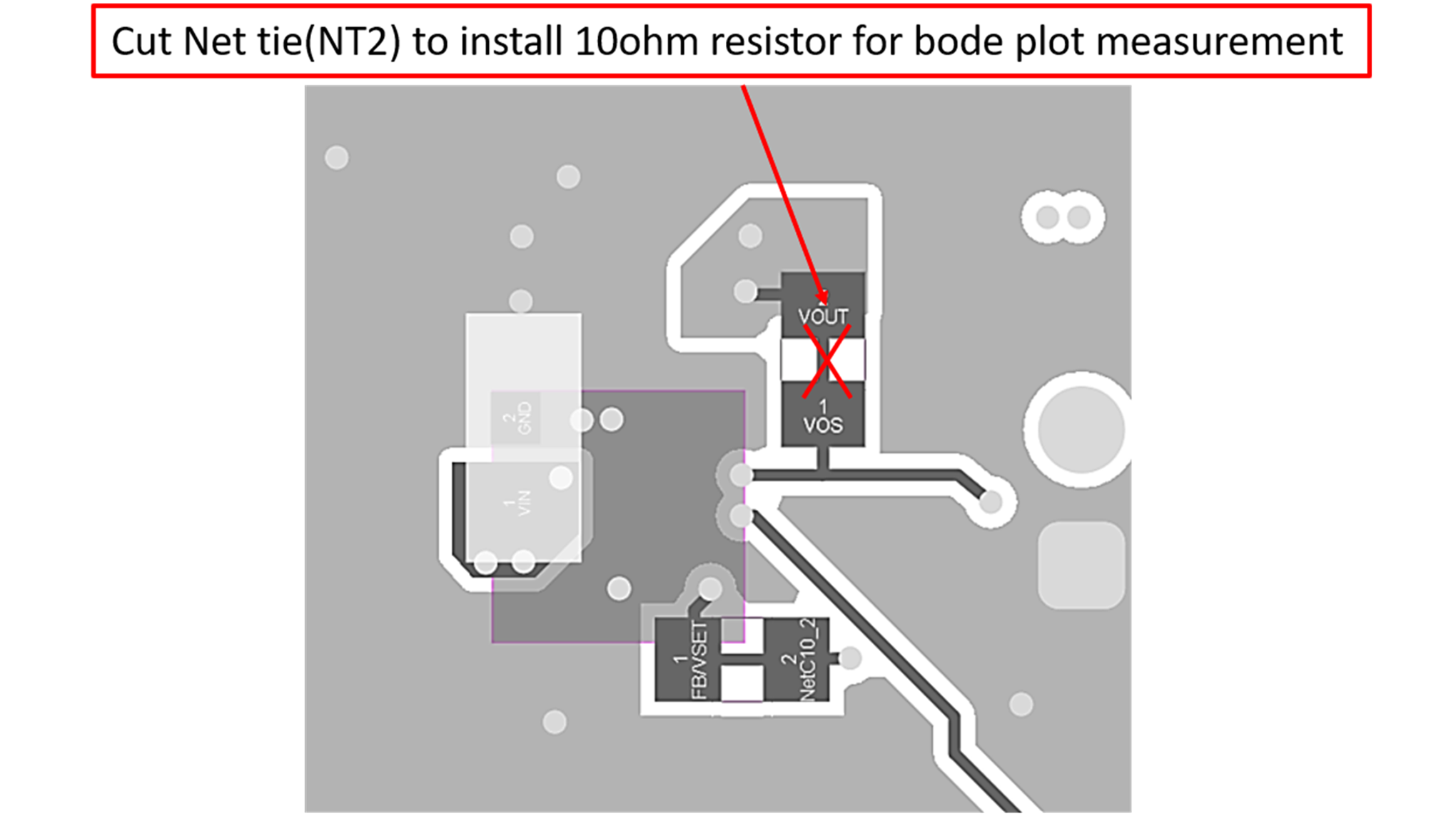
GUID-20210521-CA0I-ZJHP-Q0R5-VDDHZZ5TNWLT-low.png Figure 3-2 Bode Plot Measurement Board Modification