SLVU953A October   2013  – May 2021 TPS65580 , TPS65581


  1.   Trademarks
  2. 1Introduction
  3. 2Performance Specification Summary
  4. 3Modifications
    1. 3.1 Output Voltage Setpoint
  5. 4Test Setup and Results
    1. 4.1 Input/Output Connections
    2. 4.2 Start-Up Procedure
    3. 4.3 Efficiency
    4. 4.4 Load Regulation
    5. 4.5 Line Regulation
    6. 4.6 Load Transient Response
    7. 4.7 Input Voltage Ripple
    8. 4.8 Start-Up
  6. 5Board Layout
    1. 5.1 Layout
  7. 6Schematic, Bill of Materials, and Reference
    1. 6.1 Schematic
    2. 6.2 Bill of Materials
    3. 6.3 Reference
  8. 7Revision History

Input Voltage Ripple

The TPS65581EVM-575 input voltage ripple is shown in Figure 4-10. The output current for each channel is the full rated load of 1.5-A, 2.5-A and 1.5-A. Note that the switching waveforms for each channel are out of phase to reduce input ripple.
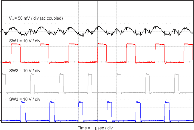
GUID-F0CEEED5-521B-4376-BEF9-DF5E7AE3306D-low.gifFigure 4-10 TPS65581EVM-575 Input Voltage Ripple