SLVU953A October   2013  – May 2021 TPS65580 , TPS65581


  1.   Trademarks
  2. 1Introduction
  3. 2Performance Specification Summary
  4. 3Modifications
    1. 3.1 Output Voltage Setpoint
  5. 4Test Setup and Results
    1. 4.1 Input/Output Connections
    2. 4.2 Start-Up Procedure
    3. 4.3 Efficiency
    4. 4.4 Load Regulation
    5. 4.5 Line Regulation
    6. 4.6 Load Transient Response
    7. 4.7 Input Voltage Ripple
    8. 4.8 Start-Up
  6. 5Board Layout
    1. 5.1 Layout
  7. 6Schematic, Bill of Materials, and Reference
    1. 6.1 Schematic
    2. 6.2 Bill of Materials
    3. 6.3 Reference
  8. 7Revision History

Load Transient Response

The TPS65581EVM-575 CH1 response to load transients is shown in Figure 4-9. The current steps and slew rates are indicated in the figures. Total peak-to-peak voltage variation is as shown. The transient response for CH2 and CH3 is similar and is not shown.
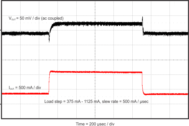
GUID-EA4151B3-09F1-427C-98B1-154C4FC60E9A-low.gifFigure 4-9 TPS65581EVM-575 CH1 Load Transient Response, 25% to 75% Load Step