SLVU953A October   2013  – May 2021 TPS65580 , TPS65581


  1.   Trademarks
  2. 1Introduction
  3. 2Performance Specification Summary
  4. 3Modifications
    1. 3.1 Output Voltage Setpoint
  5. 4Test Setup and Results
    1. 4.1 Input/Output Connections
    2. 4.2 Start-Up Procedure
    3. 4.3 Efficiency
    4. 4.4 Load Regulation
    5. 4.5 Line Regulation
    6. 4.6 Load Transient Response
    7. 4.7 Input Voltage Ripple
    8. 4.8 Start-Up
  6. 5Board Layout
    1. 5.1 Layout
  7. 6Schematic, Bill of Materials, and Reference
    1. 6.1 Schematic
    2. 6.2 Bill of Materials
    3. 6.3 Reference
  8. 7Revision History

Line Regulation

The line regulation for the TPS65581EVM-575 CH1, CH2, and CH3 is shown in Figure 4-8. Note that the CH1 output voltage is 3.3 V and the line regulation is lessened as VIN approaches VOUT.
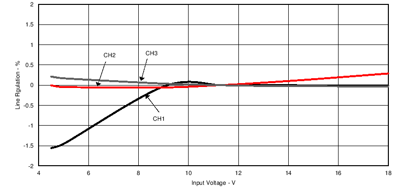
GUID-44FEA442-E46F-4F33-8634-C79579FAE2BE-low.pngFigure 4-8 TPS65581EVM-575 Line Regulation