SLVU379A August 2010 – August 2021 TPS54521
1.3.1 Output Voltage Set Point
The output voltage is set by the resistor divider network of R8 and R9. R9 is fixed at 10 kΩ. To change the output voltage of the EVM, it is necessary to change the value of resistor R8. Changing the value of R8 can change the output voltage above 0.8 V. The value of R8 for a specific output voltage can be calculated using Equation 1.
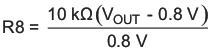
Table 1-3 lists the R8 values for some common output voltages. Note that VIN must be in a range so that the minimum on-time is greater than 135 ns, and the maximum duty cycle is less than 95%. In addition, different output voltages may require different frequency compensation, which will require changes to the values of R4, C4, C6, and C11. The values given in Table 1-3 are standard values, not the exact value calculated using Equation 1.
| OUTPUT VOLTAGE (V) | R8 VALUE (kΩ) | |
|---|---|---|
| 1.8 | 12.4 | |
| 2.5 | 21.5 | |
| 3.3 | 31.6 | |
| 5 | 52.3 | |