SLVAET8 June 2020 TPS62810-Q1 , TPS62810M , TPS62811-Q1 , TPS62811M , TPS62812-Q1 , TPS62812M , TPS62813-Q1 , TPS62813M , TPS62824A , TPS62825 , TPS62825A , TPS62826 , TPS62826A , TPS62827 , TPS62827A
2.1 Light Load Efficiency and Fast Transient Response
Texas Instruments DCS-Control topology is an advanced DC/DC converter architecture that combines the advantages of hysteretic and voltage mode control in order to provide excellent DC-voltage and load-transient regulation, low output voltage ripple, and a seamless transition from pulse-width modulation (PWM) to Power Save Mode (PSM) operation as shown in High-efficiency, low-ripple DCS-Control™ offers seamless PWM/power-save transitions article. DCS-Control devices, like the TPS6282X TPS6282x, 2.4-V to 5.5-V input, 2-, 3-, 4-A step-down converter with 1% output accuracy in 1.5-mm × 1.5-mm QFN package data sheet, can support applications where highest efficiency is required over a large output current range, and excellent transient response is required to cleanly power dynamic loads in processors, like for example the VCCINT_VCU rail.
The TPS6282X is a 2.4-V to 5.5-V input step-down converter pin-to-pin family featuring output currents ranging from 1/2-A to 4-A and available in a 1.5-mm x 1.5-mm QFN package. Some device versions include an automatically entered power save mode (PSM) to maintain high efficiency down to very light loads for extending the system battery runtime. The internal reference allows regulating the output voltage with a high feedback voltage accuracy of 1% over the junction temperature range of –40°C to 125°C.
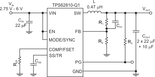
 Figure 1. Typical TPS6282X Application Circuit
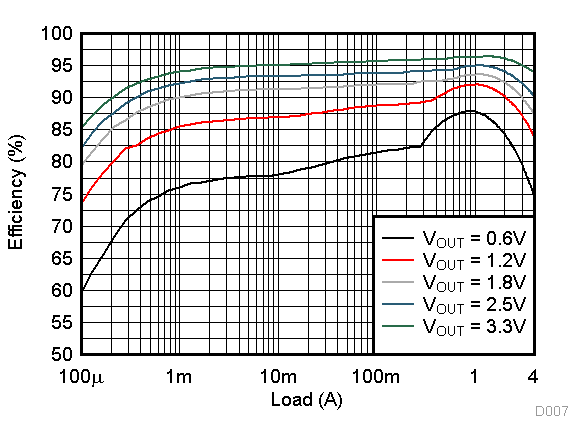
  Figure 2. Efficiency vs. Load at VIN=5V
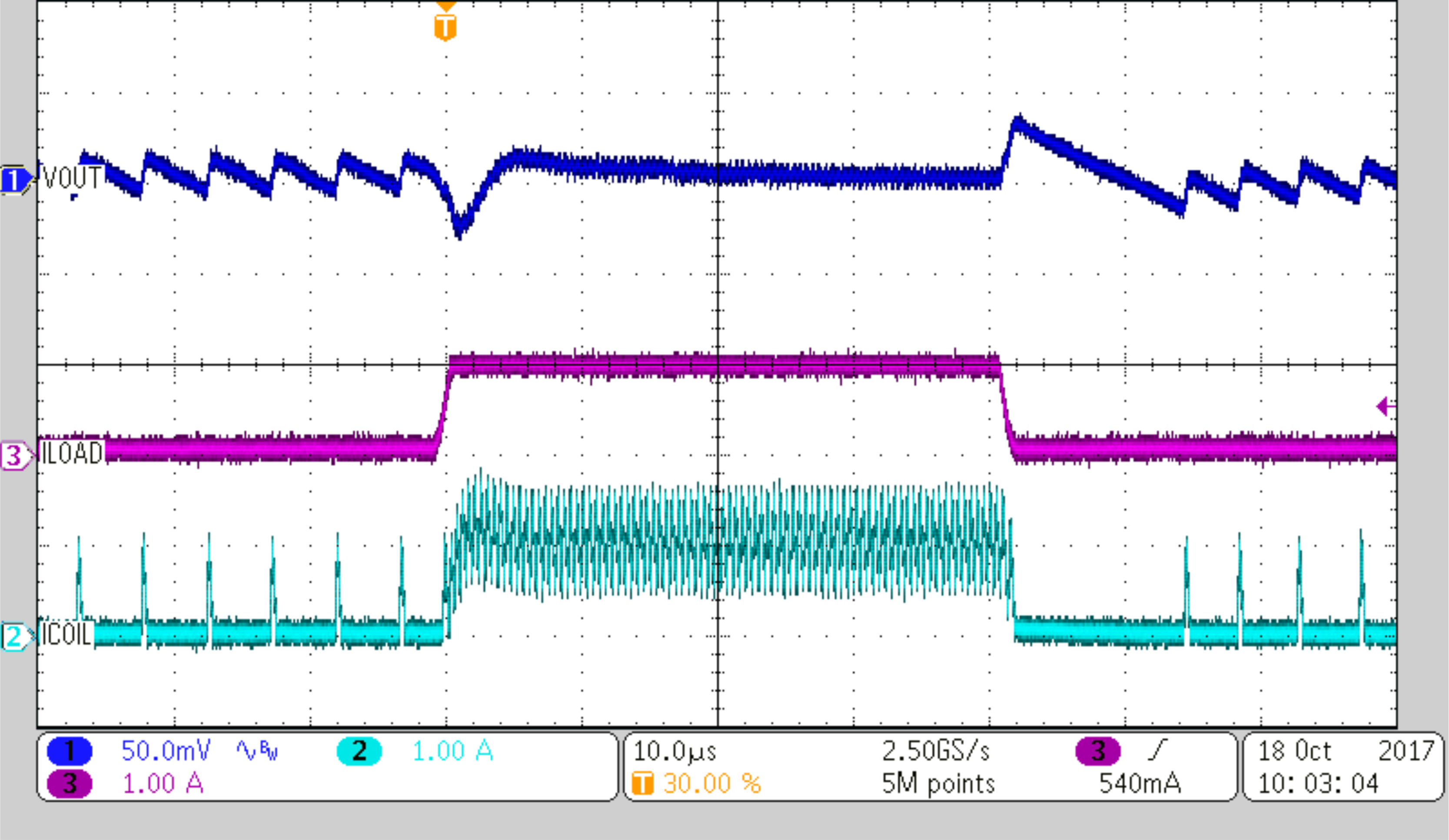
  Figure 3. Load transient Performance with Iout = 0.05A to 1A