SLVAEF0 September 2020 – MONTH TPS92630-Q1 , TPS92638-Q1
1 Introduction
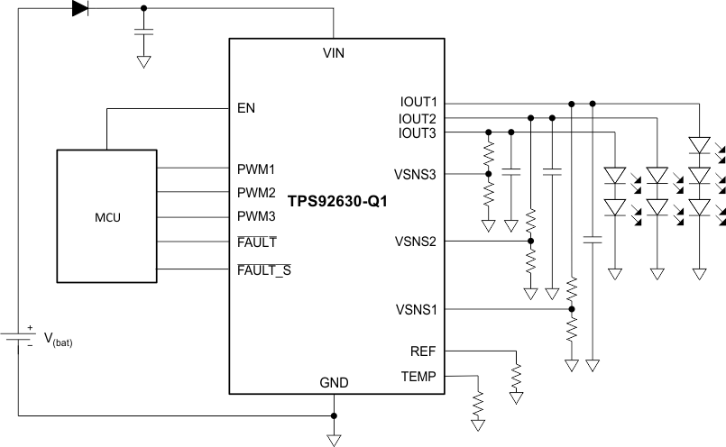
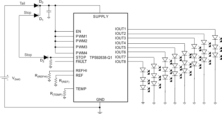
Figure 1-1 and Figure 1-2 shows the typical application schematics of the two devices. The VIN pin for TPS92630-Q1 and the SUPPLY pin for TPS92638-Q1 are power supply input pins. The voltage of the supply pins are expressed as V(supply) hereinafter. The supported supply voltage range of TPS92630/8-Q1 is 5 V - 40 V.
 Figure 1-1 TPS92630-Q1 Typical Application Schematic
 Figure 1-2 TPS92638-Q1 Typical Application Schematic
Both devices have full-diagnostic and built-in protection capabilities, such as output short-to-ground detection, open-load detection and reference resistor short detection. The fault detection features are effective when the device is enabled (V(EN) > 2 V).