SLVA416A September 2010 – September 2021 DRV8424 , DRV8812 , DRV8813 , DRV8818
3 Application Block Diagram
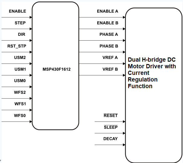
In essence, the combination portrayed in Figure 3-1is similar to how a stepper with internal indexer operates. A logic block samples a series of inputs and generates control signals to the dual H Bridge device. Typical internal indexer driver devices represent an encased application and can not be modified. However, by splitting the application into a microcontroller and a driver, more flexibility is obtained.
Figure 3-1 shows how the MSP430F1612 drives the control signals such as PHASE, ENABLE and VREF. ENABLE and PHASE signals are derived from conventional GPIO configured as outputs, whereas the VREF analog signals are derived from both of MSP430F1612’s DAC outputs. An interrupt subroutine computes the next step and generates the next microstep.
 Figure 3-1 Application Block Diagram