SLUUAS2C October 2013 – November 2021
8 EVM Assembly Drawing and PCB Layout
The following figures show the design of the TPS53915EVM-PWR587 printed circuit board (see Figure 8-1 through Figure 8-8). The EVM has been designed using a six-layer 2-oz copper-circuit board.
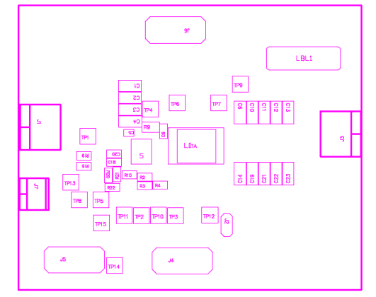 Figure 8-1 TPS53915EVM-587 Top-Layer Assembly Drawing
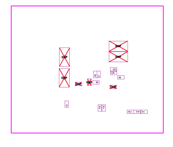 Figure 8-2 TPS53915EVM-587 Bottom-Layer Assembly Drawing
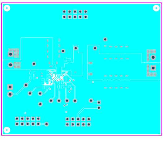 Figure 8-3 TPS53915EVM-587 Top Layer, Copper
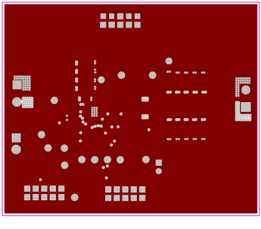 Figure 8-4 TPS53915EVM-587 Layer Two, Copper
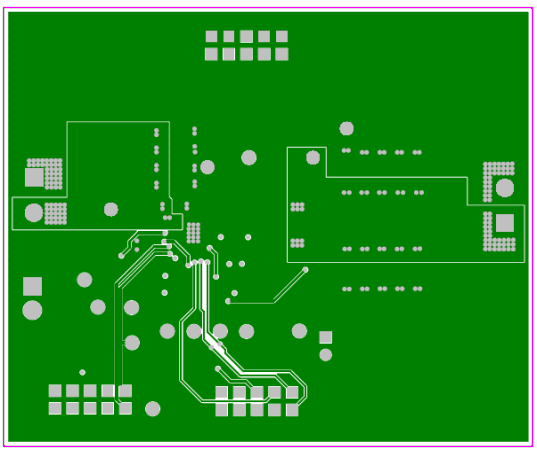 Figure 8-5 TPS53915EVM-587 Layer Three, Copper
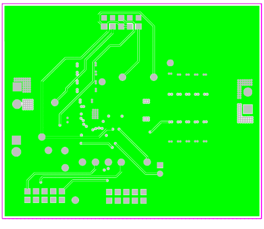 Figure 8-6 TPS53915EVM-587 Layer Four, Copper
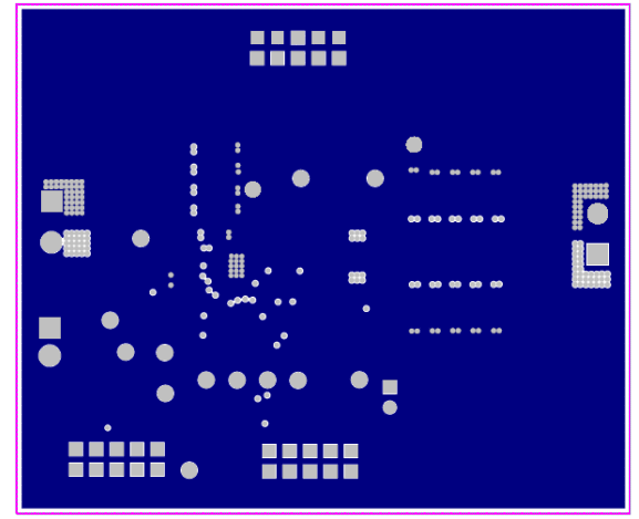 Figure 8-7 TPS53915EVM-587 Layer Five, Copper
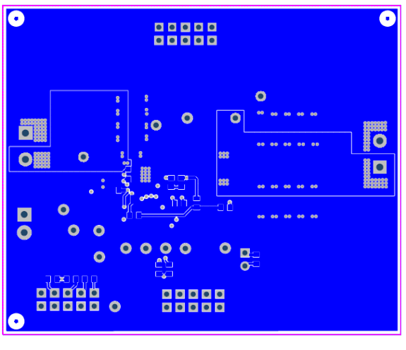 Figure 8-8 TPS53915EVM-587 Bottom Layer, Copper