SLUUAS2C October   2013  – November 2021


  1.   Trademarks
  2. 1 Introduction
  3. 2 Description
    1. 2.1 Typical Applications
    2. 2.2 Features
  4. 3 Electrical Performance Specifications
  5. 4 Schematic
  6. 5 Test Setup
    1. 5.1 Test Equipment
    2. 5.2 Recommended Test Setup
  7. 6 Configurations
    1. 6.1 PMBus Address Selection
    2. 6.2 Mode Selection
    3. 6.3 VDD Pin Supply Selection
  8. 7 Test Procedure
    1. 7.1 Line and Load Regulation and Efficiency Measurement Procedure
    2. 7.2 PMBUS Setup and Verification
    3. 7.3 Control-Loop Gain and Phase-Measurement Procedure
    4. 7.4 List of Test Points
    5. 7.5 Equipment Shutdown
  9. 8 EVM Assembly Drawing and PCB Layout
  10. 9 Bill of Materials
  11. 10Revision History

Recommended Test Setup

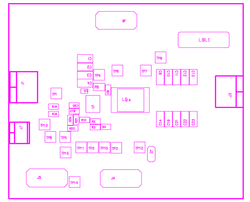
GUID-D2A490B0-0547-45DA-8715-B2BBC2BB38A2-low.gifFigure 5-2 TPS53915EVM-587 Top Layer for Test Setup

Input Connections:

  1. Prior to connecting the DC input-source, VIN, TI recommends to limit the source current from VIN to 10-A maximum. Ensure that VIN is initially set to 0 V and connected as shown in Figure 5-2.
  2. Connect the voltmeter V1 at TP1 (VIN) and TP4 (GND) to measure the input voltage.

Output Connections:

  1. Connect the load to J3 and set the load to constant-resistance-mode to sink 0-ADC before VIN is applied.
  2. Connect the voltmeter V2 at TP7 (VOUT) and TP9 (GND) to measure the output voltage.