SLUSD37E October 2017 – November 2019
PRODUCTION DATA.
- 1 Features
- 2 Applications
- 3 Description
- 4 Revision History
- 5 Device Comparison Tables
- 6 Pin Configuration and Functions
- 7 Specifications
-
8 Detailed Description
- 8.1 Overview
- 8.2 Functional Block Diagram
- 8.3
Feature Description
- 8.3.1 CrM/DCM Control Principle
- 8.3.2 Line Voltage Feed-Forward
- 8.3.3 Valley Switching and CrM/DCM Hysteresis
- 8.3.4 Transconductance Amplifier with Transient Speed-up Function
- 8.3.5 Faults and Protections
- 8.3.6 High-Current Driver
- 8.4 Controller Functional Modes
- 9 Application and Implementation
- 10Power Supply Recommendations
- 11Layout
- 12Device and Documentation Support
- 13Mechanical, Packaging, and Orderable Information
8.3.5.3.2 Second Level Over-Voltage Protection (Ovp2)
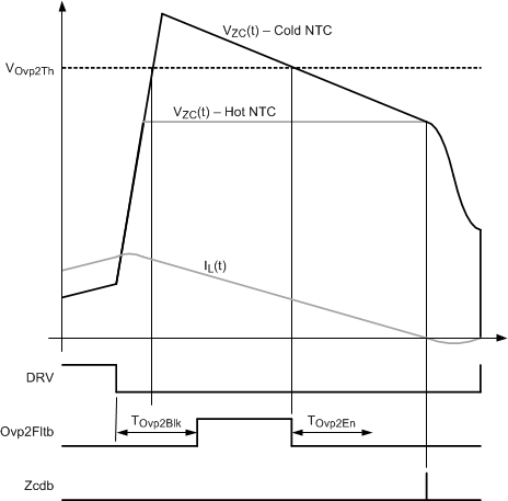
During the TDCH period when the Boost diode is conducting, (and neglecting impedance in series with the Boost diode) the voltage across the MOSFET approximates to the output voltage. The controller monitors the voltage across the MOSFET via an external divider network connected to the ZCD/CS pin. This monitoring provides a second independent method to detect excessive output voltage in case the VOSNS pin divider becomes damaged. An Ovp2 comparator with a fixed threshold (VOvp2Th) monitors the ZCD/CS pin voltage during the TDCH period. A fixed blanking period (TOvp2Blk) is applied after the falling edge of the DRV waveform to ensure that the Ovp2 comparator is not tripped by inductive spikes on the leading edge of the Drain waveform.
The UCC28056 controller can operate with an in-rush limiting NTC resistor located on the load side of the Boost MOSFET. Placing the NTC resistor in this location allows the use of a smaller controller with reduced current rating and delivers better efficiency. The voltage drop across the series resistance introduced by the NTC, particularly when cold, causes a voltage drop across the Boost MOSFET that is higher than the output voltage, for example during the early part of the TDCH period when the current flowing through the Boost diode and NTC resistor is highest. The excess voltage across the Boost MOSFET caused by the a cold NTC has two important consequences:
- It may cause the Ovp2 comparator to be tripped when the output voltage is not excessive.
- Excessive voltage stress applied to the Boost MOSFET, during a cold start, may cause it to be damaged.
The UCC28056 triggers an Ovp2 fault if the time between the falling edge of the Ovp2 comparator output and the Zcdb signal is less than TOvp2En for three consecutive switching cycles. The series impedance required to trigger a false Ovp2 fault is greatly increased because the Ovp2 comparator must be tripped close to the Zcdb point when the current flowing through the NTC resistor is small.
An internal discharge resistor (RCODisch) between the COMP and GND pins connected for each switching cycle causes the Ovp2 comparator to trip. This internal resistance discharges the external compensation network reducing power demand and therefore the peak current flowing through the NTC resistor. The internal COMP discharge resistor remains connected for any switching cycle that triggers the Ovp2 comparator. The internal COMP discharge resistor becomes disconnected after the first switching cycle that does not trigger the Ovp2 comparator. By limiting the peak current flowing through the cold NTC resistor, the effect of this circuit is to limit the peak voltage stress applied to the Boost MOSFET during a cold start.
 Figure 24. Waveforms to Illustrate Ovp2 Operation