SLUP408 February 2022 LM25149-Q1 , LM61460-Q1 , LM61495-Q1 , LMQ61460-Q1
- 1 Introduction
- 2 Defining EMI
- 3 What Causes EMI in a Switched-Mode DC/DC Regulator?
- 4 Existing Passive EMI Filtering Techniques
- 5 Passive Filter Limitations
- 6 AEF
- 7 Spread Spectrum
- 8 DRSS
- 9 True Slew-Rate Control
- 10HotRod™ Package Technology
- 11Optimized Package and Pinout
- 12Integrated Capacitors
- 13Conclusions
- 14References
- 15Important Notice
6 AEF
An AEF uses an amplifier circuit to sense noise on the input rail and inject an out-of-phase signal to cancel the noise being sensed. As shown in Figure 6-1, an operational-amplifier (op-amp) network acts effectively to replace a passive capacitor (CF) with an active capacitor. The op-amp network requires feedback and compensation components, but these components are much smaller in size and cost than a large passive CF. Integrating the op amp into a DC/DC controller package, as in the LM25149-Q1, results in a smaller overall filter size when compared to a fully passive EMI filter.
 Figure 6-1 A passive EMI filter (a); an
AEF-equivalent model (b); an AEF implementation (c).
Figure 6-1 A passive EMI filter (a); an
AEF-equivalent model (b); an AEF implementation (c).Figure 6-2 shows a more detailed view of an AEF circuit. An AEF with voltage sensing and current injection (VSCI) uses capacitive sensing and injection; therefore, it does not source or sink any DC current. The AEF cancels the AC ripple current of the input filter inductor (as illustrated in Figure 6-2, with triangular waveforms for simplicity). Consequently, the DC input current does not determine the size of the AEF; instead, it is limited by the op amp’s source-and-sink current capability, as it cancels the AC ripple current in the filter inductor. As a result, an AEF can work with high levels of DC power, with appropriate sizes of LIN and CIN to keep the input ripple and noise within the range of the op amp’s source-and-sink current capability.
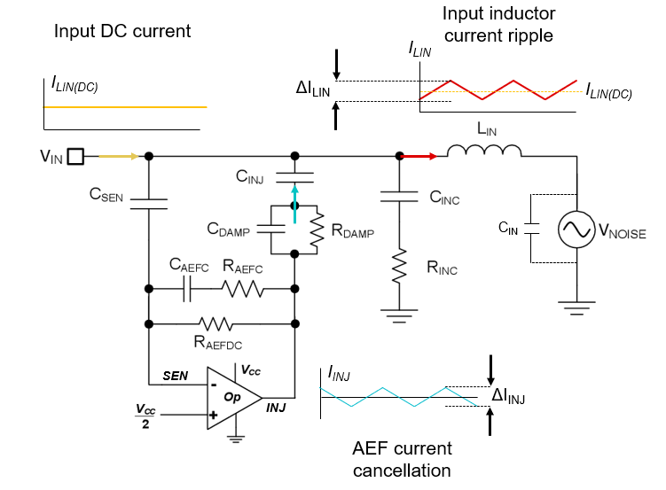 Figure 6-2 An AEF implementation in which
capacitive sensing and injection ensure that the AEF does not source or sink DC
current; as a result, the AEF size is independent of DC power, and only limited
to canceling the input inductor ripple current.
Figure 6-2 An AEF implementation in which
capacitive sensing and injection ensure that the AEF does not source or sink DC
current; as a result, the AEF size is independent of DC power, and only limited
to canceling the input inductor ripple current.The op amp forms a band-stop filter. The term GOp expresses the gain of the op amp, approximated by the active EMI sensing and compensation capacitors CSEN and CAEFC in Equation 4:
Equation 5 has the same format as Equation 3; however, CF is replaced with an injection capacitor (CINJ) and GOp. Using an AEF, you can design for a similar filter cutoff frequency or performance using much lower component values for LIN and CINJ.
For example, with GOp equal to 100, an AEF can reduce the inductance of LIN and the capacitance of CINJ by a factor of 10 for each component. Furthermore, a smaller LIN and CINJ will have lower parasitics and much higher SRFs for better high-frequency performance.
Figure 6-3 and Table 6-1 compare passive and active EMI filters. The passive filter layout uses an inductor that has a significantly larger volume. The AEF layout uses smaller and cheaper components while achieving improved filter performance. The op amp is integrated in the controller integrated circuit (IC), not shown in Figure 6-3.
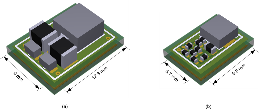 Figure 6-3 A passive EMI filter with two
1210 capacitors (a); an AEF with significantly smaller and cheaper components
(b).
Figure 6-3 A passive EMI filter with two
1210 capacitors (a); an AEF with significantly smaller and cheaper components
(b).| Passive | Active | |
|---|---|---|
| Cost | $2.71 | $1.70 |
| Area | 110.7 mm2 | 55.8 mm2 |
| Height | 5.2 mm | 4 mm |
Figure 6-4 shows the EMI performance of the regulator – without a filter, with a passive EMI filter, and with an AEF. The AEF uses smaller components for a 50% area reduction, with improved EMI attenuation.
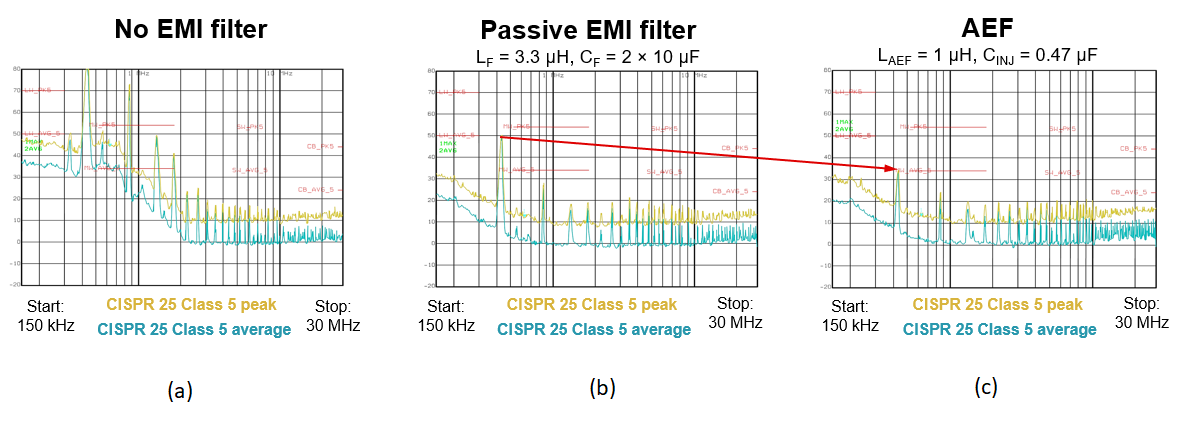 Figure 6-4 An EMI scan with no filter
(a); an EMI scan with a passive EMI filter (b); an EMI scan with an AEF
(c).
Figure 6-4 An EMI scan with no filter
(a); an EMI scan with a passive EMI filter (b); an EMI scan with an AEF
(c).It is important to carefully select active EMI components, as some components can cause resonances if you do not meet certain frequency requirements. A sensing or injection component SRF that is less than the active EMI system crossover frequency can create unintended resonance, as shown in Figure 6-5. To avoid resonances, it is recommended to have an active EMI network crossover of around 15 MHz set by input compensation resistor and capacitance RINC and CINC, and using components with an SRF of at least 15 to 20 MHz.
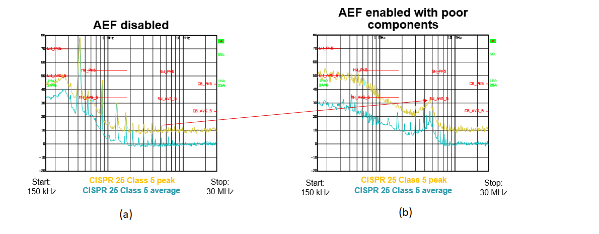 Figure 6-5 An EMI scan with no filter
(a); an EMI scan with an AEF using a low-quality injection capacitor with a
component SRF of 5 MHz (b).
Figure 6-5 An EMI scan with no filter
(a); an EMI scan with an AEF using a low-quality injection capacitor with a
component SRF of 5 MHz (b).Component layout is an important consideration for AEFs. Keep loop areas formed by circuits small and away from noise sources, and connected directly to a ground plane where large currents are not flowing. At the op-amp IC, place the VCC decoupling capacitor very close to the VCC and power GND pins. Ensure that the AEF amplifier is grounded directly to the ground plane where high currents are not flowing. Keeping the loop area small, route the SEN and INJ traces tightly together from the amplifier.
As shown in Figure 6-6, the SEN and INJ traces should connect directly at compensation components RAEFC, CAEFC and RAEFDC in the blue square. Place the sensing CSEN close to the compensation and the injection-damping network RDAMP, CDAMP and CINJ on the opposite side of sensing, as shown in the red and yellow squares. Finally, be sure that the input compensation CINC and RINC connect to quiet GND, as shown in the purple squares.
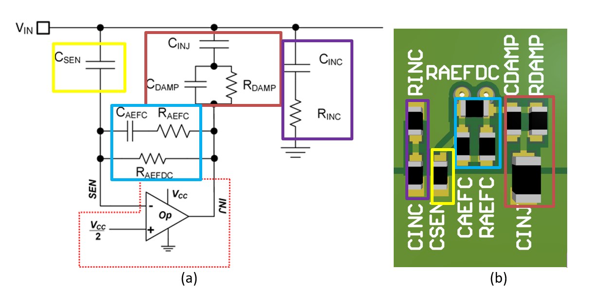 Figure 6-6 Active EMI schematic (a);
suggested layout (b).