SLUAAC0 September 2021 TPS92519-Q1 , TPS92520-Q1
1.1 TPS92520-Q1
The TPS92520-Q1 can be programed using SPI, so that each channel is an independent constant current, synchronous buck output. There are a variety of registers that control output current setpoints: switching frequency, PWM control, and modes of operation. There are also registers that give information on the status of the device and other measurements, such as input voltage and output voltage.
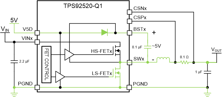
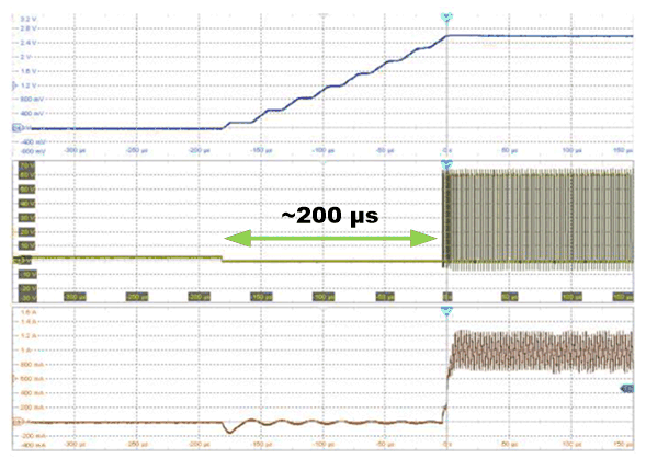
The device has a floating gate driver that depends on charging the BST cap by turning on the Low-Side FET (LS-FET), which creates a 5-V supply that is floating on the switch node and drives the High-Side FET (HS-FET). The TPS92520-Q1 turns on the LS-FET for approximately 200 µs during the initial start-up to perform the initial charge of the BST cap and is constantly charged by the switching action of the buck converter during steady state operation. See Figure 1-3 and Figure 1-4.
 Figure 1-3 BSTx Capacitor Charging at Start-up
 Figure 1-4 Start-up Waveform for a Single Channel
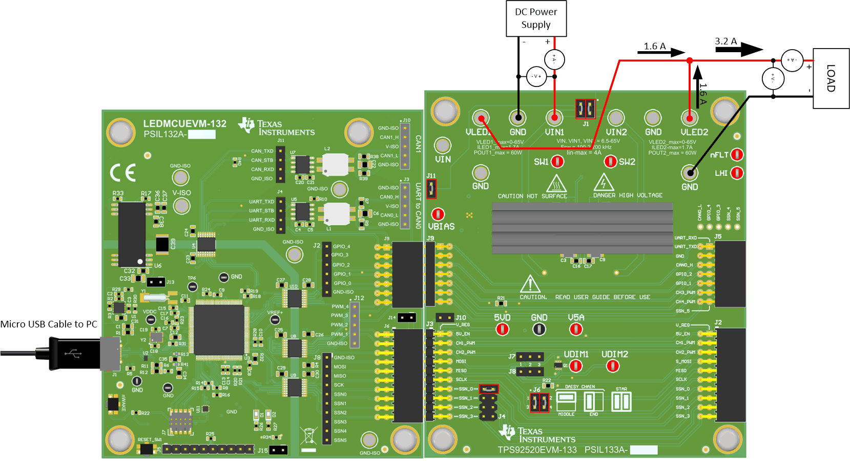
Achieving 3.2 A of output current is as simple as connecting the two output channels together and ensuring that both channels perform their start-up sequence at the same time. See Figure 1-5.
 Figure 1-5 Parallel Connection of Outputs Using the TPS92520EVM-133 and LEDMCUEVM-132 Controller
Synchronization of the start-up sequence is achieved by turning on both channels at the same time (CH1EN and CH2EN bits) by performing a single write to the SYSCFG1 register (address 0x00h). If using the internal PWM registers to perform PWM dimming, then the PWM phase bit (PWMPH) must be set to 1 to establish 0 phase shift between both channels. See Figure 1-6.
 Figure 1-6 CH1EN, CH2EN, and PWMPH Bits in SYSCFG1 Register (0x00h)
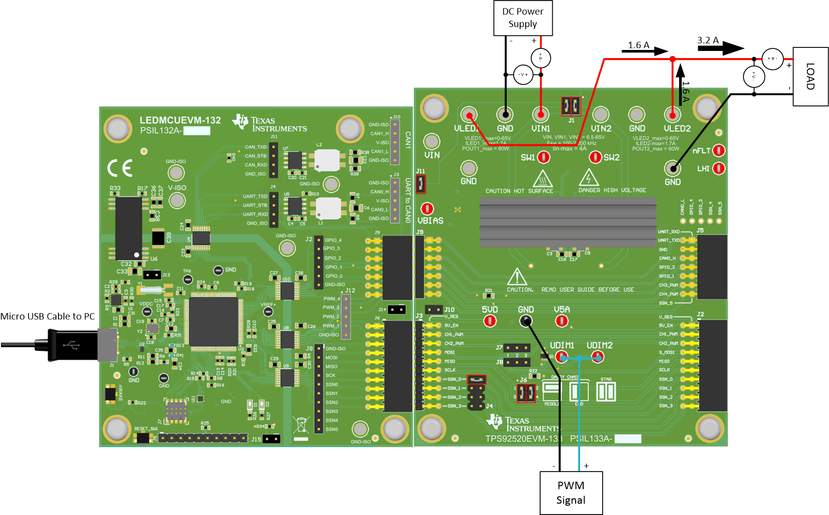
If external PWM dimming is performed using the UDIM pints, then the signals to UDIM1 and UDIM2 pins must be tied together or be precisely controlled so that they are synchronized with very small delays. Figure 1-7 shows external PWM signal from external source and not the LEDMCUEVM-132 board’s external PWM signals (PWM-1 and PWM-2). See LEDMCUEVM-132 User’s Guide for more details.
 Figure 1-7 PWM Dimming Using External Signals to UDIM1 and UDIM2 Pins