SLUA748A December 2015 – April 2016 BQ25120 , BQ51003 , TPS61046 , TPS61240 , TPS62743
- Trademarks
- Power Management Reference Design for a Wearable Device with Wireless Charging Using the bq51003 and bq25120
- AExperimental Results
- Revision History
A.1 Experimental Results
Efficiency of Wireless Input Stage. The figure shows the efficiency across the power range with the bq51003. This is the total DC/DC system efficiency including the transmitter, coils and receiver. Testing was done with the TIDA-00334 Small Form Factor Transmitter reference design (5-V input) and the TDK WR222230-26M8-G coil. The TIDA-00334 reference design is pictured below with the results.
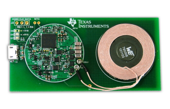 Figure 13. TIDA-00334 Board
 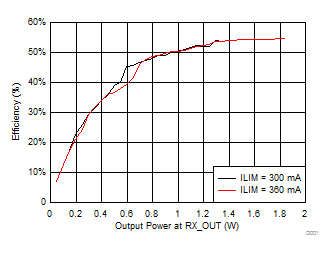 Figure 14. Wireless Power Efficiency
 Figure 15 and Figure 16 show the efficiency and load regulation of the bq25120 1.8V buck output with a 3.8V VBAT input. For full performance data of the BQ25120, see the datasheet.
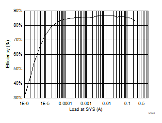 Figure 15. BQ25120 Buck Efficiency
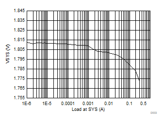 Figure 16. BQ25120 Buck Load Regulation
Figure 17 and Figure 18 show the efficiency and load regulation of the TPS62743 1.8 V Buck Output from a 3.8V VBAT input. The input to the TPS62743 is connected to PMID, so the efficiency includes the drop through the bq25120 battery discharge FET. For full performance data of the TPS62743, see the datasheet.
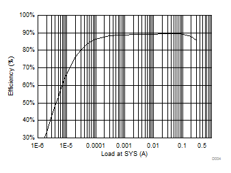 Figure 17. TPS62743 Buck Efficiency
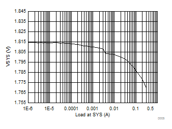 Figure 18. TPS62743 Buck Load Regulation
Figure 19 and Figure 20 show the efficiency and load regulation of the TPS61046 12 V Boost Output from a 3.8V VBAT input. The input to the TPS61046 is connected to PMID, so the efficiency includes the drop through the bq25120 battery discharge FET. For full performance data of the TPS61046, see the datasheet.
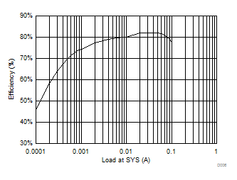 Figure 19. TPS61046 Boost Efficiency
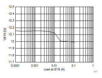 Figure 20. TPS61046 Boost Load Regulation
Figure 21 and Figure 22 show the efficiency and load regulation of the TPS61240 5 V Boost Output from a 3.8V VBAT input. The input to the TPS61240 is connected to PMID, so the efficiency includes the drop through the bq25120 battery discharge FET. For full performance data of the TPS61240, see the datasheet.
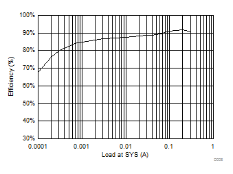 Figure 21. TPS61240 Boost Efficiency
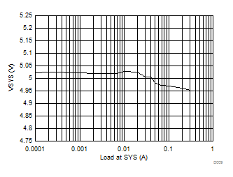 Figure 22. TPS61240 Boost Load Regulation
The following thermal images are of the board with various outputs and loads applied.
Table 2. Board Outputs and Loads
| BQ25120 SYS | BQ25120 LS/LDO | TPS61046 BOOST 12V | TPS61240 BOOST 5V | TPS62743 V_BUCK | CURRENT FROM VBAT (A) | (1) BOARD MAX TEMP °C | (2) BQ25120 MAX TEMP °C | AMBIENT TEMP °C | |
|---|---|---|---|---|---|---|---|---|---|
| Image 1 | 200 mA | 0 mA | 0 mA | 0 mA | 0 mA | 0.11117 | 27.08 | 25.28 | 22.5 |
| Image 2 | 200 mA | 100 mA | 0 mA | 0 mA | 0 mA | 0.20982 | 28.08 | 26.58 | 22.5 |
| Image 3 | 200 mA | 100 mA | 100 mA | 0 mA | 0 mA | 0.67541 | 57.72 | 37.95 | 22.5 |
| Image 4 | 200 mA | 100 mA | 100 mA | 200 mA | 0 mA | 1.0723 | 69.2 | 53.51 | 22.5 |
| Image 5 | 200 mA | 100 mA | 100 mA | 200 mA | 200 mA | 1.19482 | 80.79 | 64.66 | 22.5 |
| Image 6 | 0 mA | 0 mA | 0 mA | 0 mA | 0 mA | 0.000041 | 24.47 | 23.29 | 22.5 |
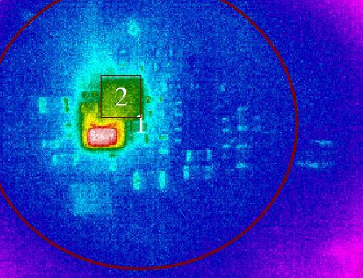 Figure 23. Image 1
 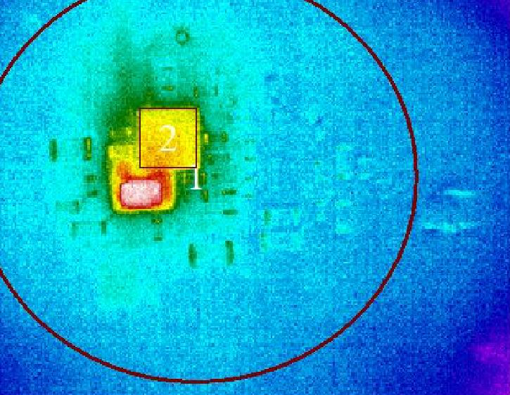 Figure 24. Image 2
 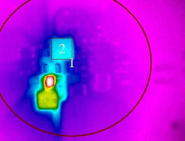 Figure 25. Image 3
 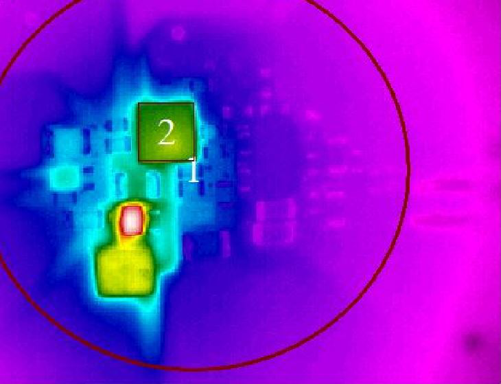 Figure 26. Image 4
 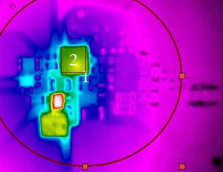 Figure 27. Image 5
 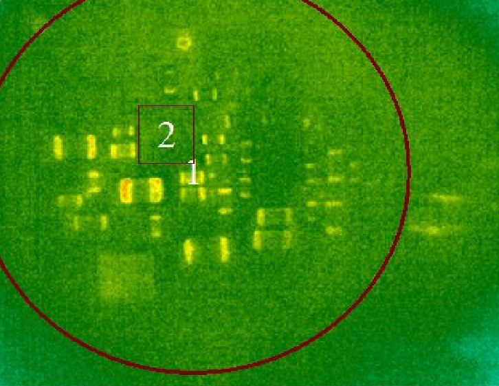 Figure 28. Image 6
 Table 3. Board Outputs and Loads
| BQ51003 | BQ25120 SYS | BQ25120 LS/LDO | TPS61046 BOOST 12 V | TPS61240 BOOST 5 V | TPS62743 V_BUCK | (1) BQ25120 MAX TEMP °C | (2) BQ51003 MAX TEMP °C | AMBIENT TEMP °C | |
|---|---|---|---|---|---|---|---|---|---|
| Image 7 | On | 100 mA Fast Charge | Off | Off | Off | Off | 31.7 | 32.18 | 22.5 |
| Image 8 | On | 200 mA Fast Charge | Off | Off | Off | Off | 39.66 | 34.31 | 22.5 |
| Image 9 | On | 300 mA Fast Charge | Off | Off | Off | Off | 35.13 | 38.52 | 22.5 |
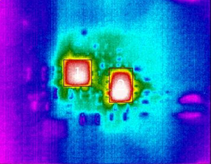 Figure 29. Image 7
 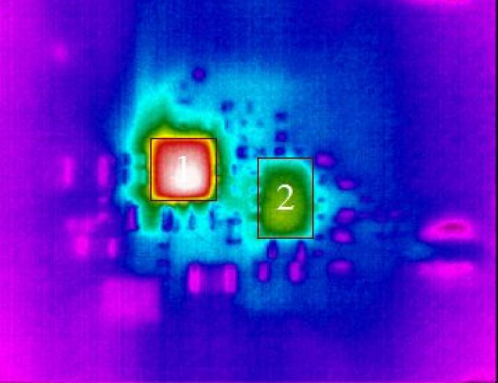 Figure 30. Image 8
 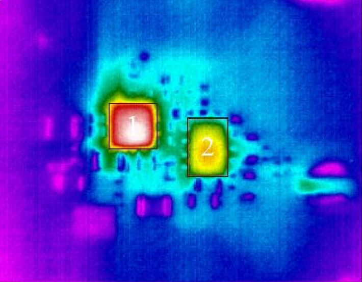 Figure 31. Image 9