SLUA748A December 2015 – April 2016 BQ25120 , BQ51003 , TPS61046 , TPS61240 , TPS62743
- Trademarks
- Power Management Reference Design for a Wearable Device with Wireless Charging Using the bq51003 and bq25120
- AExperimental Results
- Revision History
4.4 Boost Converters (TPS61046 and TPS61240)
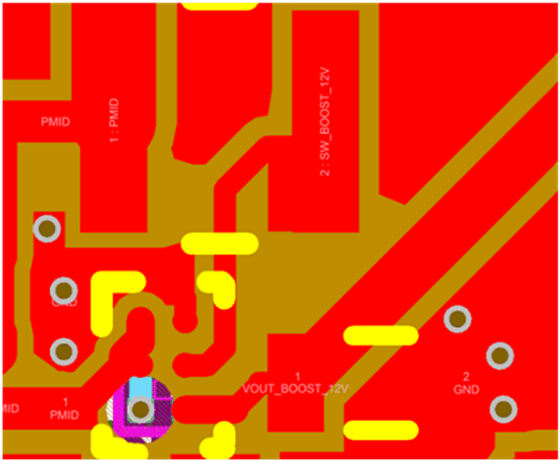
- The switching node should be as short as possible.
- It is recommended to place the input capacitor close not only to the VIN and GND pins.
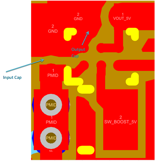
- The output capacitor must be placed close to the IC and it is recommended to be close to the ground pin. If possible, the ground for the input and output capacitor should be on the same plane. In the TPS61046 it was not possible to follow this rule due to the placement for reduced size. Therefore, a solid ground with vias was provided on the next layer making sure the connection is adequate.
 Figure 10. Capacitor Grounding TPS61046
  Figure 11. TPS61240 Layout