SLLU356 September 2022 THVD1424
3.1.1.3 Default Operation Mode
With an understanding of how the board is setup and how to power the board for both supply situations the next topic is how to operate the board. Out of the box the board, when powered, can operate the THVD1424 as a full or half duplex RS-485 transceiver. The devices pins can be broken down into 4 distinct groups: single ended communication pins, differential communication pins, power pins, and control pins. Power pins are discussed above in the previous section, section 3.3, details below for the other 3 categories.
The single ended communication pins are to be connected directly, through their respective jumpers, to a single ended bus – these pins are the “R” and “D” pins and represent RX and TX single ended data respectively. R is connected to J1 and D is connected to J4 – these are the console side signal connection points for the EVM.
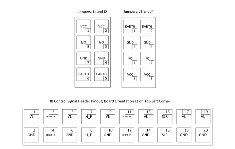
The THVD1424 has six control pins that vary in function. Two signals are enable signals for the driver (DE – active high) and receiver (/RE – active low) that are accessed through J3 and J2 respectively. The other four control signals are TERM_TX, H/F, TERM_RX, and the SLR pins which can be accessed through J8 and have internal pull-downs leaving a default state as logic low on these four pins. A jumper configuration for J1 – J4 and J8 are shown in Figure 3-1 with board orientation having jumper J1 at the top left corner of the board. A function table for the control signals are shown in Table 3-4
 Figure 3-1 Control Signal Jumper
Configuration
Figure 3-1 Control Signal Jumper
Configuration| Pin | Associated Jumper - Pin | Input Level | Function |
|---|---|---|---|
| RE | J2-3 and J2-8 | Hi | Receiver Disabled |
| RE | J2-3 and J2-8 | Low | Receiver Enabled |
| DE | J3-4 and J3-7 | Hi | Driver Enabled |
| DE | J3-4 and J3-7 | Low | Driver Disabled |
| TERM-TX | J8-3 and J8-4 | Hi | Y-Z Termination Enabled |
| TERM-TX | J8-3 and J8-4 | Low | Y-Z Termination Disabled |
| H/F | J8-7 and J8-8 | Hi | Half Duplex Mode |
| H/F | J8-7 and J8-8 | Low | Full Duplex Mode |
| TERM-RX | J8-11 and J8-12 | Hi | A-B Termination Enabled |
| TERM-RX | J8-11 and J8-12 | Low | A-B Termination Disabled |
| SLR | J8-15 and J8-16 | Hi | 500Kbps Mode |
|
SLR |
J8-15 and J8-16 | Low | 20Mbps Mode |
Finally, the last group of signals are the differential bus pins A, B, Y, and Z. A and B are connected at terminal J14 with Y and Z at terminal J17. In Half Duplex Mode Y and Z are both the TX and RX connections, in full duplex mode A and B are receiver pins and Y and Z are transmission pins.