SLIB006A February 2011 – June 2021 TPS81256 , TPS82084 , TPS82085 , TPS82130 , TPS82140 , TPS82150 , TPS82670 , TPS82671 , TPS826711 , TPS826716 , TPS82672 , TPS826721 , TPS82673 , TPS82674 , TPS826745 , TPS82675 , TPS82676 , TPS826765 , TPS82677 , TPS8268090 , TPS8268105 , TPS8268120 , TPS8268150 , TPS8268180 , TPS82692 , TPS82693 , TPS82695 , TPS826951 , TPS82697 , TPS82698 , TPS82740A , TPS82740B , TPSM82810 , TPSM82813 , TPSM82816 , TPSM82821 , TPSM82821A , TPSM82822 , TPSM82822A , TPSM82823 , TPSM82823A
4 Surface Mount Assembly
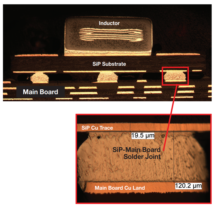
Surface mounting of MicroSiP BGA and LGA packages is broadly similar to BGA and QFN package assembly, respectively. TI recommends the use of lead-free solder paste applied via a 0.1-mm thick stencil. The paste acts to aid wetting of the MicroSiP pin to the board land pad, to hold the device in place during reflow, and to contribute metal volume of the resultant solder joint. For the setup of a reflow profile, the JEDEC reflow profiles for near-eutectic SnAgCu solder alloys can be used as a starting point with soldering temperatures up to 250°C. The resulting solder joint height is typically around 120 µm. Figure 4-1 shows a cross-section of solder joints which attach three BGA pins to a four-layer PCB.

Figure 4-1 Cross-Section of a MicroSiP™ With BGA Pins on Top of a Four-Layer PCB
All MicroSiP devices passed BLR testing during their development. As an example, 8-pin MicroSiP devices with BGA pins were assembled after preconditioning with no underfill or adhesive used. Table 4-1 shows the BLR test results.
| Test Parameters | Results (tfirst fail) | |
|---|---|---|
| Drop | 1500 G, 1.0 ms pulse | > 100 drops |
| Temperature Cycle | –40, 125°C, 2 cycles/hr | > 1000 cycles |
The surface mounting process of MicroSiP devices with LGA pins is similar to a QFN package assembly. Irregular surface plating, uneven solder paste thickness, and crowning of the solder plating can reduce overall surface mounting yields. Bare copper with an organic solderability preservative (OSP) coating, tin (Sn) plating or electro-less nickel immersion gold (ENIG) have been shown to provide an acceptable land pad surface.
The advantages of plating over OSPs are better shelf life, permanent coverage of copper vias and other features not exposed to a solder process, and contamination resistance. Even with these differences, OSPs have shown robust performance in the industry. In summary, a controlled assembly process for soldering MicroSiP devices with LGA pins package relies on a flat, uniform PCB pad surface. Achieving a flat, uniform surface leads to a greater control of solder paste uniformity, resulting in an overall robust process. See the QFN and SON PCB Attachment application report for more details on soldering QFN packages.
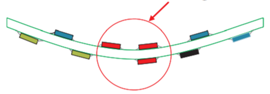
As explained in the QFN and SON PCB Attachment application report, all devices (including MicroSiPs) need to be placed carefully to avoid regions of extreme deflection, if the PCB will be subject to excessive bending during manufacturing. Excessive bending of the PCB can lead to package damage and should be avoided in the assembly flow.

Figure 4-2 Avoid Excessive Bending