SLAA220A November 2004 – August 2018 MSP430F423 , MSP430F423 , MSP430F423A , MSP430F423A , MSP430F425 , MSP430F425 , MSP430F425A , MSP430F425A , MSP430F427 , MSP430F427 , MSP430F427A , MSP430F427A
2 Hardware Description
To address the outlined application requirements, an integrated MCU solution is used. The MSP430F42xA ultra-low-power flash-based microcontrollers include 3 integrated 16-bit sigma-delta analog-to-digital converters (SD16). These data converters also feature an on-chip programmable gain amplifier (PGA) that allows the amplification of incoming signals up to 32 times. The bridge sensor is connected directly to the microcontroller. Section 4 shows the schematic of the board that was used to develop this application.
The negative excitation signal of the full-bridge sensor is connected to terminal X1-1, and the positive excitation signal is connected to terminal X1-4. These terminals are powered trough MCU port pins P2.0 and P2.1, respectively. The bridge excitation voltage can be disabled to reduce power consumption between measurements or when the weight scale is operated in standby mode. With a bridge resistance of 1200 Ω (typical) and a supply voltage of 3 V, the sensor consumes 2.5 mA when excited. The bridge sensor output signals are connected to X1-2 and X1-3, passed through two low-pass filters, and fed into the SD16 input channel A0.
The particular full-bridge sensor that is used has a rated full-scale output voltage of 2 mV/V when loaded with its maximum load capacity of approximately 10 kg. The design goal is to resolve the sensor signal with a resolution of 1 g, resulting in a total of 10000 counts, and display the weight on an LCD. The entire application is powered from a 3-V battery source. If the bridge sensor is excited with 3 V, it delivers a full-scale output voltage of 3 V × 2 mV/V = 6 mV. This also means that 1 g equals a voltage of 6 mV / 10 kg × 1 g = 0.6 µV. To resolve 1 g, the LSB voltage of the ADC should be four times smaller that, which is 0.6 µV / 4 = 0.15 µV.
The MSP430 SD16 16-bit sigma-delta ADC can operate using either a built-in reference of 1.2 V or an externally connected reference voltage. This application uses the external reference. An external resistor divider provides the reference voltage. With the bridge sensor powered from the same voltage source, this configuration has the advantage of implementing a VCC-independent ratiometric measurement principle. If the bridge sensor were to be powered from VCC and use the internal voltage reference for the SD16 module, the measurement results would change as VCC changes over the lifetime of the battery. Using the resistor divider and a supply voltage of 3 V, the reference voltage is as follows:

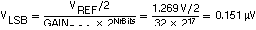
The R9/R10 divider ratio was chosen so that the generated reference voltage stays in the allowed VREF(I) range, while VCC drops from 3 V to 2.7 V. The minimum supply voltage for the SD16 module is 2.7 V. For detailed SD16 voltage ranges and other parameters, see the MSP430F42xA data sheet. The SD16 reference voltage determines the full-scale differential input voltage, which is VREF/2. As the data converter is bipolar, the ADC LSB voltage is:

By using the maximum PGA gain of 32, the LSB voltage decreases to 0.605 µV. This is still approximately 4 times higher than the design goal of 0.15 µV. An external op-amp could be used to provide this additional amplification. Another approach without adding external components is to use additional SD16 output bits. The SD16 module is a 16-bit ADC, but it provides access to a total of 24 bits from its internal digital decimation filter. By adding two more of the bits from the digital filter output to the 16-bit conversion result and low-pass filtering this 18-bit output signal by averaging multiple results, the LSB voltage reduces to 0.151 µV.
With this voltage, the resolution requirement can be fulfilled, even though the full-scale sensor output voltage is only 6 mV and the full input range of the sigma-delta converter is not used.
The MSP430F427A on-chip LCD driver directly interfaces to common LCDs. This application uses the SBLCDA4, a 4-mux 7.1-digit LCD from SoftBaugh. Resistors R5, R7, and R8 provide the voltage ladder for the LCD driver module. A 32-kHz watch crystal is the system clock reference to drive the LCD display and to provide periodic wakeup from low-power modes during application operation. A push button (SW1) to start the weight scale operation connects to P1.0.