SCDA039 October 2021 TMUX7308F , TMUX7309F , TMUX7412F , TMUX7462F
1 Overvoltage and Overstress Events and Effects
An overvoltage event can be defined as an event where the voltage seen at one or more of the device inputs exceeds the absolute maximum rating as defined in the data sheet. The traditional CMOS switch structure as shown in Figure 1-1 can help illustrate how an overvoltage event occurs.
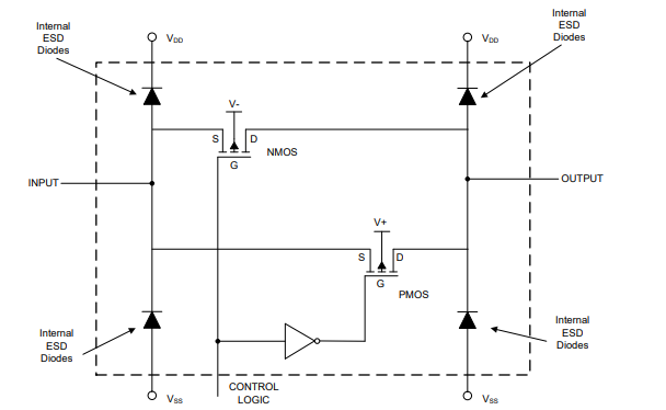 Figure 1-1 CMOS Switch
Architecture
Figure 1-1 CMOS Switch
ArchitectureIn many multiplexers and signal switches, there are ESD diodes tied between the input and the positive supply rail (VDD/VCC) and an ESD diode tied from the input to the negative supply rail or ground (VSS/GND). The purpose of these ESD diodes is to protect against ESD HBM and CDM events that can often be encountered during the manufacturing process or just in general handling of the device. Now, these diodes will begin conduction when they have a forward voltage drop of around 0.4V-0.7V and can sustain only a certain amount of current going through them for a limited amount of time. When an overvoltage event occurs, this will cause these diodes to turn on and begin conducting a very large current that will inevitably damage these diodes as there is normally no current limiting resistor in the path. Figure 1-2 is an illustration of such an overvoltage event:
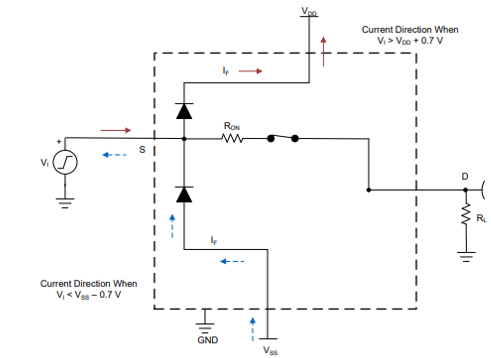 Figure 1-2 ESD Diode Conduction during
Overvoltage Event
Figure 1-2 ESD Diode Conduction during
Overvoltage EventIn addition, the device that is directly in the signal chain of the overvoltage event is not the only device at risk. Any devices that are also powered by the same supply rail or are referenced to the same ground can be affected as well. This phenomenon is known as backpowering. Backpowering can be described using the Figure 1-3.
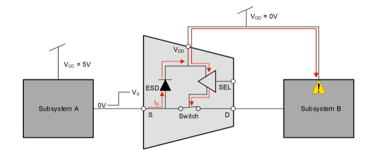 Figure 1-3 Backpowering during an
Overvoltage Event
Figure 1-3 Backpowering during an
Overvoltage EventAs shown in Figure 1-3, the overvoltage signal can be passed through the power rail to other devices downstream, potentially powering them up to a higher voltage than expected which can cause unexpected behavior in the system or can damage the devices.
Overstress events, like a hard short, can also introduce a potentially hazardous environment to the device as well. In most data sheets, there is a limited continuous current a multiplexer device can sustain before there is a risk to damaging the device. This risk is due to the power dissipation the device can handle and varies depending on the architecture of the switch, rated maximum voltage, package, and PCB design. Without any current limiting resistors or built-in current clamps to the device, these events can be particularly catastrophic to the system and can destroy multiple devices along the fault path.
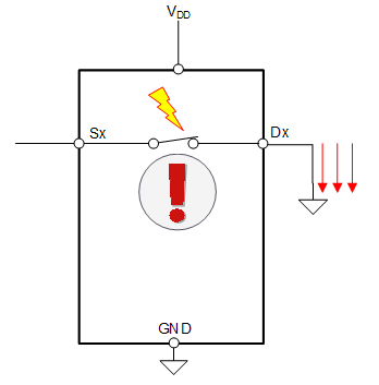 Figure 1-4 Short Circuit Fault
Lastly, ground shifting and common mode faults are other sources of possible system overstress. Ground shifting is when the circuit common reference is altered from its original or intended state and can be inadvertently introduced when there are large return currents flowing through the system (such as during an overcurrent event). Ideally, the system should have all the ground paths connected to one point (known as a star connection), however if not implemented, ground shifting can cause a significant impact on the system. Figure 1-5 is an example.
In the scenario above, it is evident that connecting each subsystem to ground at a different point can easily introduce differences in ground references between circuits. This is due to the fact that as the return current traverses through the return path, the different resistances and currents at each branch cause fluctuations in the ground reference of each circuit.
As stated previously, if the return current is large enough, it can shift the ground reference enough that it could cause the device to be exposed to an overvoltage event. Common mode faults are similar in which the ground reference suddenly changes to create an unsafe environment for the device, but occurs in a different way. Figure 1-7 illustrates an example.
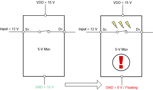 Figure 1-7 Common Mode Fault
Note that in this example, the GND is being referenced to 10 V and VDD is being referenced to 15 V, hence the device is operating as a 5 V device since that is what the device sees as a potential difference. Now, what happens if the 10V supply faults or gets shorted? This fault or short would cause the device to suddenly see the full 15 V and would cause a significant overvoltage event that would ultimately damage the device. While using ground shifting and common mode voltages can create great flexibility in a system, they are prone to these types of faults that can be catastrophic to the system if not implemented properly.