SBOS562G August 2011 – June 2020 INA826
PRODUCTION DATA.
- 1 Features
- 2 Applications
- 3 Description
- 4 Revision History
- 5 Device Comparison Table
- 6 Pin Configuration and Functions
- 7 Specifications
-
8 Detailed Description
- 8.1 Overview
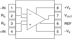
- 8.2 Functional Block Diagram
- 8.3 Feature Description
- 8.4 Device Functional Modes
- 9 Application and Implementation
- 10Power Supply Recommendations
- 11Layout
- 12Device and Documentation Support
- 13Mechanical, Packaging, and Orderable Information
6 Pin Configuration and Functions
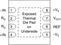
DRG Package
8-Pin WSON
Top View

Pin Functions
| PIN | I/O | DESCRIPTION | ||
|---|---|---|---|---|
| NAME | NO. | |||
| SOIC, VSSOP | WSON | |||
| –IN | 1 | 1 | I | Negative (inverting) input |
| +IN | 4 | 4 | I | Positive (noninverting) input |
| REF | 6 | 6 | I | Reference input. This pin must be driven by low impedance. |
| RG | 2 | 2 | — | Gain setting pin. Place a gain resistor between pin 2 and pin 3. |
| 3 | 3 | |||
| VOUT | 7 | 7 | O | Output |
| –VS | 5 | 5 | — | Negative supply |
| +VS | 8 | 8 | — | Positive supply |
| Thermal pad | — | — | — | Exposed thermal die pad is internally connected to –VS. Connect externally to –VS or leave floating. |
