SBOA442 March 2021 TMP107 , TMP107-Q1
3 TMP107-Q1 Over the CAN Bus
The CAN transceiver has dedicated pins for receiving (RXD) and transmitting (TXD) data. The TMP107-Q1 sensor has a single bidirectional pin (I/O). Connecting the bidirectional pin I/O directly to the RXD and TXD pins is not possible. The CAN transceiver has an internal loopback that mirrors all data on the CAN bus to the RXD pin. Merging RXD and TXD pins together would result in the bus conflict with undefined behavior.
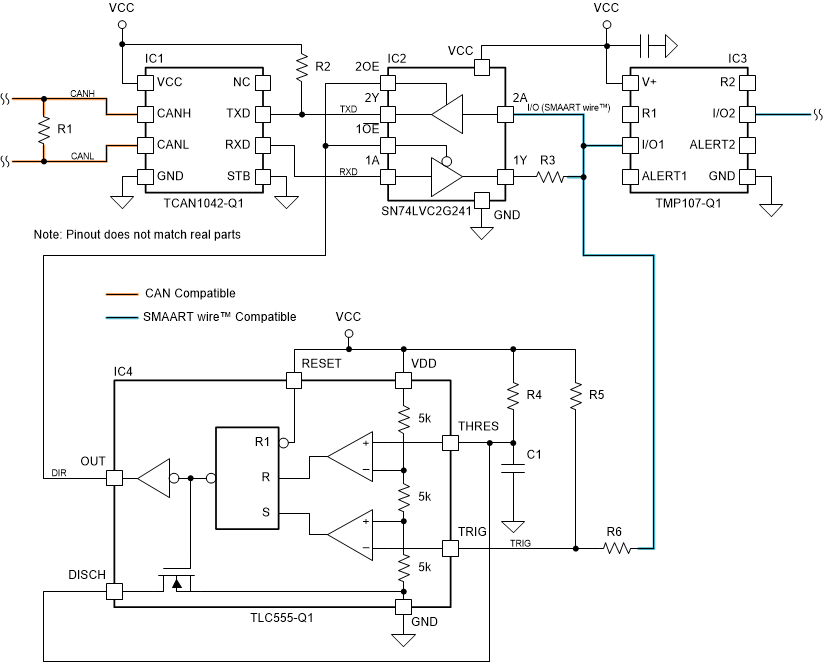
 Figure 3-1 Simplified Circuit Diagram
for Interfacing the TMP107-Q1 Over the CAN bus
Figure 3-1 Simplified Circuit Diagram
for Interfacing the TMP107-Q1 Over the CAN busFigure 3-1 shows a circuit that allows interfacing the TMP107-Q1 sensor over the CAN bus. Two logic buffers in IC2 convert the single bidirectional I/O signal to unidirectional RXD and TXD signals. Buffer enable pins 1OE and 2OE are complementary and share the same input signal (DIR). This means only one buffer is active at the same time. This functionality allows for data direction control and prevents the bus conflict due to the loopback mechanism in the CAN transceiver IC1. When the DIR signal is low, the TMP107-Q1 sensor IC3 listens to the CAN bus. When the DIR signal is high, the sensor transmits data to the master device over the CAN bus.
The TMP107-Q1 device does not have any dedicated pin that indicates receiving or transmitting state. An external circuit detects when the sensor needs to send data and toggles the buffer IC2 accordingly. The external circuit uses the industry standard 555 timer. Alternatively an analog comparator can perform the same functionality.
The detection mechanism uses different voltage levels for the logic 0 on the SMAART wire bus interface. Only the logic 0 is important because this corresponds to the dominant state on the CAN bus.
Logic zero from the CAN bus to the SMAART wire™ bus interface
Careful selection of resistors R3, R5, R6 ensures that a logic zero on the 1Y pin of IC2 never causes voltage on the TRIG pin of the IC4 reaching the triggering threshold VCC/3. Additionally, a proper combination of resistors R3, R6 sets the voltage on the SMAART wire bus interface below the low-level input voltage (VIL) threshold. This way the sensor still detects logic 0.
Logic zero from the SMAART wire™ bus interface to the CAN bus
The TMP107-Q1 device asserts logic 0. This factors out the resistor R3 and voltage on the TRIG pin reaches the triggering threshold VCC/3. The OUT pin of the IC4 toggles high and enables the buffer IC2 for transmission. Without the optional capacitor C1 the output remains high only as long as the TRIG signal is below the threshold. This means that the pull-up resistor R2 maintains logic 1 on the TXD pin. The capacitor C1 can extend the OUT pulse duration for the complete frame. This is beneficial for higher transfer speeds when the pull-up resistor R2 may not be able to quickly bring the TXD pin to logic 1.
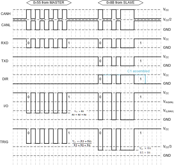
Figure 3-2 shows example waveforms for the CAN to SMAART wire interface converter circuit from Figure 3-1.
 Figure 3-2 Ideal Waveforms for the
CAN to SMAART wire™ Interface
Figure 3-2 Ideal Waveforms for the
CAN to SMAART wire™ InterfaceConverter Circuit (Example Only)