SBOA412 August 2020 TLV314-Q1
4.1 SC70-5 Package
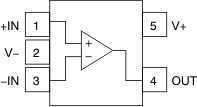
Figure 4-1 shows the TLV314-Q1 pin diagram for the SC70-5 package. For a detailed description of the device pins please refer to the Pin Configuration and Functions section in the TLV314-Q1 data sheet.
 Figure 4-1 Pin Diagram (SC70-5) Package
| Pin Name | Pin No. | Description of Potential Failure Effect(s) | Failure Effect Class |
|---|---|---|---|
| +IN | 1 |
Input at V- (GND) is valid input, however, desired application result is unlikely. Output goes low if -IN is greater than zero volts. |
B |
|
V- | 2 |
Normal operation, unless dual supply voltage was intended. |
D |
| -IN | 3 |
Input at V- (GND) is valid input, however, desired application result is unlikely. Output goes high if +IN is greater than zero volts. | C |
| OUT | 4 | May cause device to overheat. | B |
| V+ | 5 | Diodes from input to V+ may turn on due to input signal and cause electrical overstress (EOS). Main supply shorted. No power to device. | B |
| Pin Name | Pin No. | Description of Potential Failure Effect(s) | Failure Effect Class |
|---|---|---|---|
| +IN | 1 | Floating input, circuit will likely not function as expected. Output may be high or low. |
C |
|
V- | 2 |
Lowest voltage pin will drive V- pin internally via internal diode. |
B |
| -IN | 3 | Floating input, circuit will likely not function as expected. Output may be high or low. |
C |
| OUT | 4 | Output cannot be used by application. |
C |
| V+ | 5 | Highest voltage pin will drive V+ pin internally via internal diode. | B |
| Pin Name | Pin No. | Shorted to | Description of Potential Failure Effect(s) | Failure Effect Class |
|---|---|---|---|---|
| +IN | 1 |
V- | Input at V- (GND) is valid input, however, desired application result is unlikely. Output goes low if -IN is greater than zero volts. | C |
|
V- | 2 | -IN |
Input at V- (GND) is valid input, however, desired application result is unlikely. Output goes high if +IN is greater than zero volts. | C |
|
-IN | 3 | OUT |
Op amp configured as unity gain buffer. Pins are not adjacent to each other. | C |
| OUT | 4 | V+ | Output shorted to supply. May cause device to overheat. | B |
|
V+ | 5 | +IN | Input at V+ is valid input, however, desired application result is unlikely. Output goes high if -IN is less than V+. Pins are not adjacent to each other. | C |
| Pin Name | Pin No. | Description of Potential Failure Effect(s) | Failure Effect Class |
|---|---|---|---|
| +IN | 1 | Input at V+ is valid input, however, desired application result is unlikely. Output goes high if -IN is less than supply. | C |
|
V- | 2 |
Main supply shorted to V- (GND). No power to device. | C |
| -IN | 3 | Input at V+ is valid input, however, desired application result is unlikely. Output goes low if +IN is less than supply. | C |
| OUT | 4 | May cause device to overheat. | B |
| V+ | 5 | Normal operation if V+ is equal to supply. | D |