SBAA461 December 2020 ADC3541 , ADC3542 , ADC3543 , ADC3544 , ADC3641 , ADC3642 , ADC3643 , ADC3644 , ADC3660 , ADC3681 , ADC3682 , ADC3683
2.2.2 1 Wire
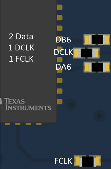
In 1 Wire mode, all 14 bits of one channel are being transmitted on one wire. With the DCLK and FCLK, this is a total of 4 output pins/resistors.
 Figure 2-7 ADC3643 Serial CMOS: 1 Wire
Resistors
Figure 2-7 ADC3643 Serial CMOS: 1 Wire
ResistorsA total of 14 bits on one wire will be transmitted over one frame clock period, so the serialization rate is 14x times the sampling rate. The data rate is limited to ~250 Mbps due to the CMOS interface, so the max sampling rate in this mode is 35 MSPS. Higher sampling rates can be used when decimation is used.
Table 2-5 1 Wire Serial CMOS (No
Decimation)
| Mode | Max Sampling Rate (MSPS) | Serialization Rate | Data Rate (Mbps) | Data Outputs/ Resistors |
|---|---|---|---|---|
| 1 Wire | 17.8 | 14 | 250 | 4 |
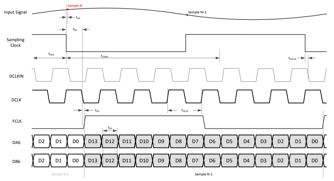
 Figure 2-8 Serial CMOS 1W Timing
Diagram