SBAA461 December 2020 ADC3541 , ADC3542 , ADC3543 , ADC3544 , ADC3641 , ADC3642 , ADC3643 , ADC3644 , ADC3660 , ADC3681 , ADC3682 , ADC3683
2.1.2 Parallel DDR
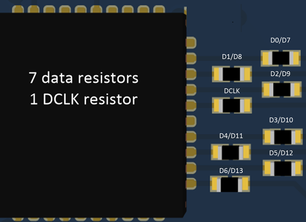
In DDR mode, two data bits correspond to one CMOS output pin on the ADC. Considering the same 14 bit ADC, only 7 data output pins (plus the DCLK) are required, halving our resistor count to 8 resistors.
 Figure 2-3 Parallel CMOS: 14 bit DDR
resistors
Figure 2-3 Parallel CMOS: 14 bit DDR
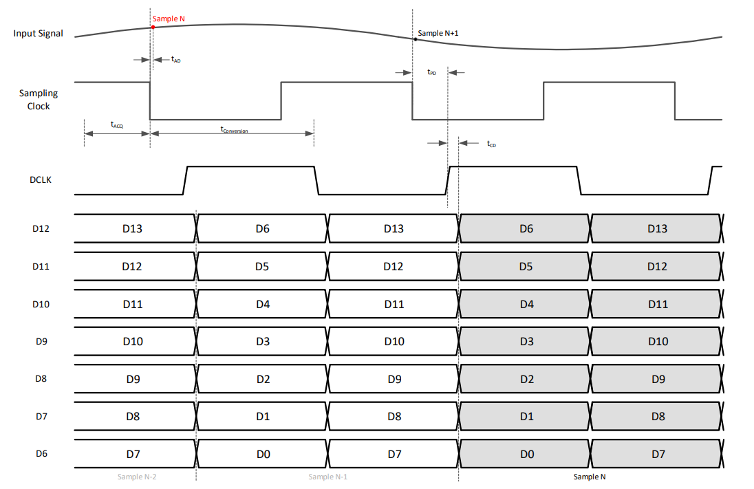
resistorsAlso the DCLK will latch the data on the rising and falling edge of the DCLK. This means that the data bits are toggling twice as fast as the DCLK. For example, if the ADC3541 is sampling at 10 MSPS, the data bits are toggling at a frequency of 20 MHz, and the DCLK is toggling at a frequency of 10 MHz.
| Parallel Interface | Max Sampling Rate (MSPS) | Data Rate (Mbps) | Data Pins/Resistors |
|---|---|---|---|
| DDR | 65 | 130 | 8 |
 Figure 2-4 Parallel CMOS DDR Timing
Diagram
Figure 2-4 Parallel CMOS DDR Timing
DiagramIn summary of the parallel interfaces, we can see that, while SDR mode offers the lowest data rate, it also requires the highest number of data output pins (resistors), and will then have a greater size/cost impact in terms of components and FPGA/uC resources. DDR mode, on the other hand, reduces the number of data output pins (resistors), but increases the data rate by a factor of 2.
| Parallel Interface | Max Sampling Rate (MSPS) | Data Rate (Mbps) | Data Outputs/Resistors |
|---|---|---|---|
| SDR | 65 | 65 | 15 |
| DDR | 65 | 130 | 8 |