SWRS070B March 2008 – September 2014 CC2591
PRODUCTION DATA.
1 Device Overview
1.1 Features
- Seamless Interface to 2.4-GHz Low-Power RF Devices from Texas Instruments
- Output Power up to 22 dBm
- Few External Components
- Integrated Switches
- Integrated Matching Network
- Integrated Balun
- Integrated Inductors
- Integrated PA
- Integrated LNA
- Digital Control of LNA Gain by HGM Pin
- 100-nA in Power Down (EN = PAEN = 0)
- Low Transmit Current Consumption
(100 mA at 3 V for 20-dBm Out, PAE = 33%) - Low-Receive Current Consumption
- 3.4 mA for High-Gain Mode
- 1.7 mA for Low-Gain Mode
- 4.8-dB LNA Noise Figure, Including T/R Switch and External Antenna Match
- RoHS Compliant 4×4-mm QFN-16 Package
- 2-V to 3.6-V Operation
1.2 Applications
- All 2.4-GHz ISM Band Systems
- Wireless Sensor Networks
- Wireless Industrial Systems
- IEEE 802.15.4 and ZigBee® Systems
- Wireless Consumer Systems
- Wireless Audio Systems
1.3 Description
CC2591 is a cost-effective and high-performance RF front end for low-power and low-voltage 2.4-GHz wireless applications. The device is a range extender for all existing and future 2.4-GHz low-power RF transceivers, transmitters, and System-on-Chip products from TI. CC2591 increases the link budget by providing a power amplifier for increased output power, and an LNA with low noise figure for improved receiver sensitivity. The device provides a small size, high output power RF design with its 4-mm × 4-mm QFN-16 package. The device contains PA, LNA, switches, RF-matching, and balun for simple design of high-performance wireless applications.
1.4 Functional Block Diagram
Figure 1-1 shows the functional block diagram of the device.
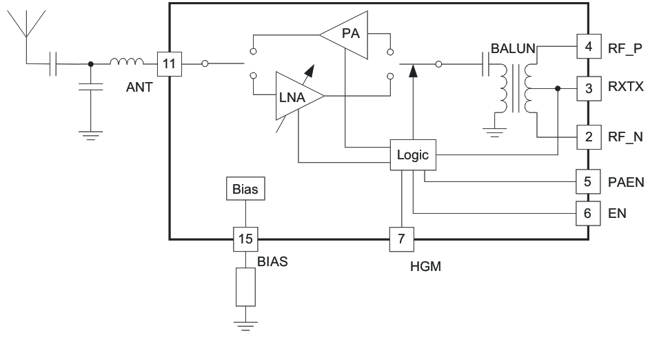 Figure 1-1 Functional Block Diagram