SWRS070B March 2008 – September 2014 CC2591
PRODUCTION DATA.
5 Applications, Implementation, and Layout
NOTE
Information in the following applications sections is not part of the TI component specification, and TI does not warrant its accuracy or completeness. TI’s customers are responsible for determining suitability of components for their purposes. Customers should validate and test their design implementation to confirm system functionality.
5.1 CC2591EM Evaluation Module
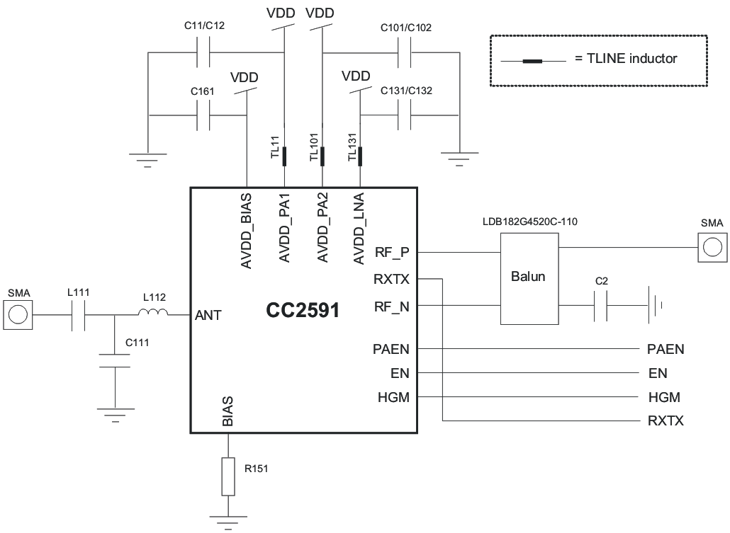 Figure 5-1 CC2591EM Evaluation Module
Table 5-1 List of Materials (See CC2591EM Reference Design)
| DEVICE | FUNCTION | VALUE |
|---|---|---|
| L112 | Part of antenna match. | 1.5 nH: LQW15AN1N5B00 from Murata |
| L111 | DC block. | 1 nF: GRM1555C1H102JA01 from Murata |
| C111 | Part of antenna match. | 1 pF: GRM1555C1H1R0BZ01 from Murata |
| C161 | Decoupling capacitor. | 1 nF: GRM1555C1H102JA01 from Murata |
| C11/C12 | Decoupling. Will affect PA resonance. | 10 pF || 1 nF. The smallest cap closest. See CC2591EM reference design (SWRU190) for placement. 10 pF: GRM1555C1H100JZ01 from Murata 1 nF: GRM1555C1H102JA01 from Murata |
| C101/C102 | Decoupling. Will affect PA resonance. | 18 pF || 1 nF. The smallest cap closest. See CC2591EM reference design (SWRU190) for placement. 18 pF: GRM1555C1H180JZ01 from Murata 1 nF: GRM1555C1H102JA01 from Murata |
| C131/C132 | Decoupling. Will affect PA resonance. | 10 pF || 1 nF. The smallest cap closest. See CC2591EM reference design (SWRU190) for placement. 10 pF: GRM1555C1H100JZ01 from Murata 1 nF: GRM1555C1H102JA01 from Murata |
| C2 | Decoupling of external balun | 1 nF: GRM1555C1H102JA01 from Murata |
| TL11 | Transmission line. Will affect PA resonance. | See CC2591EM reference design. |
| TL101 | Transmission line. Will affect PA resonance. | See CC2591EM reference design. |
| TL131 | Transmission line. Will affect LNA resonance. | See CC2591EM reference design. |
| R151 | Bias resistor | 4.3 kΩ: RK73H1ETTP4301F from Koa |
5.2 Controlling the Output Power from CC2591
The output power of CC2591 is controlled by controlling the input power. The CC2591 PA is designed to work in compression (class AB), and the best efficiency is reached when a strong input signal is applied.
5.2.1 Input Levels on Control Pins
The four digital control pins (PAEN, EN, HGM, RXTX) have built-in level-shifting functionality, meaning that if the CC2591 is operating from a 3.6-V supply voltage, the control pins will still sense 1.6-V - 1.8-V signals as logical ‘1’.
An example of the above would be that RXTX is connected directly to the RXTX pin on CC24xx, but the global supply voltage is 3.6 V. The RXTX pin on CC24xx will switch between 0 V (RX) and 1.8 V(TX), which is still a high enough voltage to control the mode of CC2591.
The input voltages should however not have logical ‘1’ level that is higher than the supply.
5.2.2 Connecting CC2591 to a CC24xx Device
Table 5-2 Control Logic for Connecting CC2591 to a CC24xx Device
| PAEN = EN | RXTX | HGM | MODE OF OPERATION |
|---|---|---|---|
| 0 | X | X | Power Down |
| 1 | 0 | 0 | RX Low Gain Mode |
| 1 | 0 | 1 | RX High Gain Mode |
| 1 | 1 | X | TX |
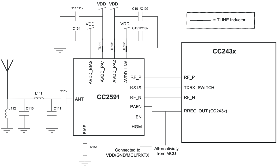 Figure 5-2 CC2591 + CC24xx Application Circuit
5.2.3 Connecting CC2591 to the CC2500, CC2510, or CC2511 Device
Table 5-3 Control Logic for Connecting CC2591 to a CC2500/10/11 Devices
| PAEN | EN | RXTX | HGM | MODE OF OPERATION |
|---|---|---|---|---|
| 0 | 0 | NC | X | Power Down |
| 0 | 1 | NC | 0 | RX LGM |
| 0 | 1 | NC | 1 | RX HGM |
| 1 | 0 | NC | X | TX |
| 1 | 1 | NC | X | Not allowed |
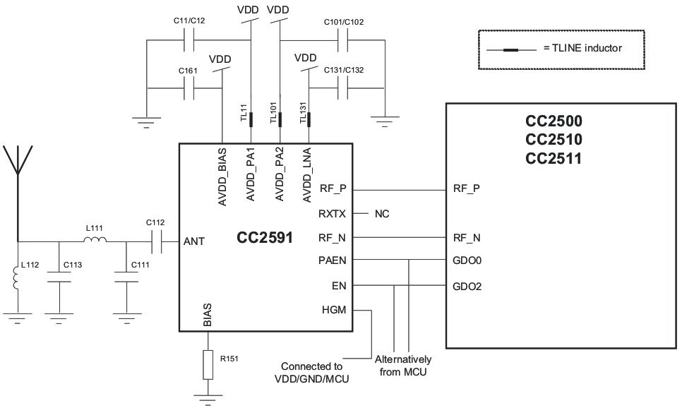 Figure 5-3 CC2591 + CC2500/10/11 Device Application Circuit
5.2.4 Connecting CC2591 to a CC2520 Device
Table 5-4 Control Logic for Connecting CC2591 to a CC2520 Device
| PAEN | EN | RXTX | HGM | MODE OF OPERATION |
|---|---|---|---|---|
| 0 | 0 | NC | X | Power Down |
| 0 | 1 | NC | 0 | RX LGM |
| 0 | 1 | NC | 1 | RX HGM |
| 1 | 0 | NC | X | TX |
| 1 | 1 | NC | X | Not allowed |
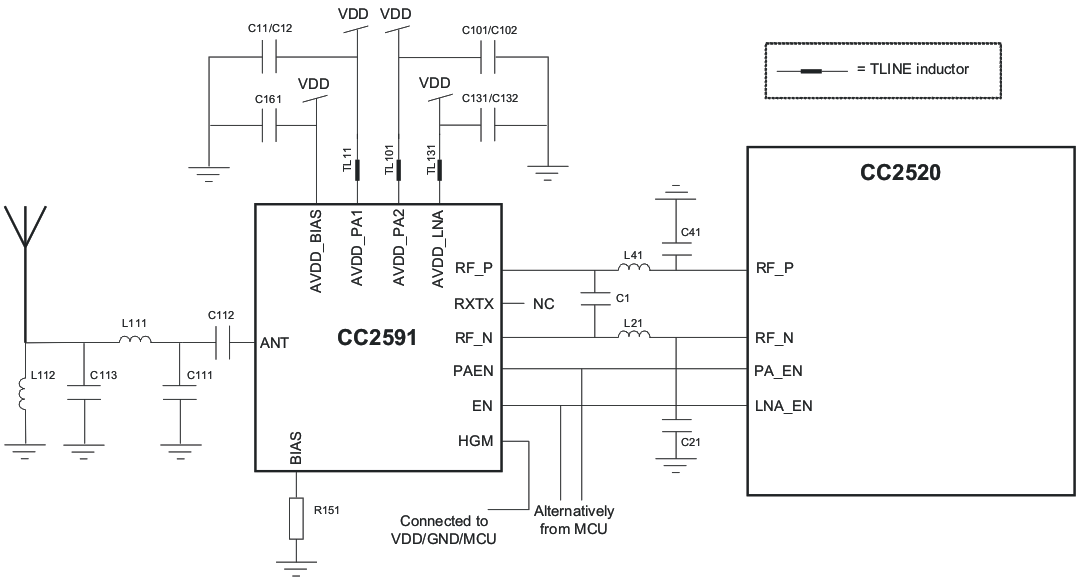 Figure 5-4 CC2591 + CC2520 Application Circuit