SWRS070B March 2008 – September 2014 CC2591
PRODUCTION DATA.
4 Specifications
4.1 Absolute Maximum Ratings(1)(2)
Under no circumstances must the absolute maximum ratings be violated. Stress exceeding one or more of the limiting values may cause permanent damage to the device.| PARAMETER | VALUE | UNIT | |
|---|---|---|---|
| Supply voltage | All supply pins must have the same voltage | –0.3 to 3.6 | V |
| Voltage on any digital pin | –0.3 to VDD + 0.3, max 3.6 | ||
| Input RF level | 10 | dBm | |
(1) Stresses beyond those listed under absolute maximum ratings may cause permanent damage to the device. These are stress ratings only, and functional operation of the device at these or any other conditions beyond those indicated under recommended operating conditions is not implied. Exposure to absolute-maximum-rated conditions for extended periods may affect device reliability.
(2) All voltage values are with respect to VSS, unless otherwise noted.
4.2 Handling Ratings
| MIN | MAX | UNIT | ||||
|---|---|---|---|---|---|---|
| Tstg | Storage temperature range | –50 | 150 | °C | ||
| VESD | Electrostatic discharge (ESD) performance: | Human Body Model (HBM), per ANSI/ESDA/JEDEC JS001(1) | –600 | 600 | V | |
| Charged Device Model (CDM), per JESD22-C101(2) |
–500 | 500 | V | |||
(1) JEDEC document JEP155 states that 500-V HBM allows safe manufacturing with a standard ESD control process.
(2) JEDEC document JEP157 states that 250-V CDM allows safe manufacturing with a standard ESD control process.
4.3 Recommended Operating Conditions
The operating conditions for CC2591 are listed below.| PARAMETER | MIN | MAX | UNIT | |
|---|---|---|---|---|
| Ambient temperature range | –40 | 85 | °C | |
| Operating supply voltage | 2 | 3.6 | V | |
| Operating frequency range | 2400 | 2483.5 | MHz | |
4.4 Electrical Characteristics
TC = 25°C, VDD = 3 V , fRF= 2440 MHz (unless otherwise noted). Measured on CC2591EM reference design including external matching components.| PARAMETER | TEST CONDITIONS | MIN | TYP | MAX | UNIT |
|---|---|---|---|---|---|
| Receive current, High-Gain Mode | HGM = 1 | 3.4 | 4 | mA | |
| Receive current, Low-Gain Mode | HGM = 0 | 1.7 | 2 | ||
| Transmit current | PIN = 0.5 dBm | 112 | |||
| Transmit current | No input signal | 40 | 50 | ||
| Power-down current | EN = PAEN = 0 | 0.1 | 0.3 | μA | |
| High-input level (control pins) | EN, PAEN, HGM, RXTX | 1.3 | VDD | V | |
| Low-input level (control pins) | EN, PAEN, HGM, RXTX | 0.3 | |||
| Power down - Receive mode switching time | 12 | μs | |||
| Power down - Transmit mode switching time | 1 | μs | |||
| RF Receive | |||||
| Gain, High-Gain Mode | HGM = 1 | 11 | dB | ||
| Gain, Low-Gain Mode | HGM = 0 | 1 | dB | ||
| Gain variation, 2400 – 2483.5 MHz, High-Gain Mode | HGM = 1 | 1.3 | dB | ||
| Gain variation, 2.0 V – 3.6 V, High-Gain Mode | HGM = 1 | 1.5 | dB | ||
| Gain variation, -40°C – 85°C, High-Gain Mode | HGM = 1 | 3 | dB | ||
| Noise figure, High-Gain Mode | HGM = 1, including internal T/R switch and external antenna match | 4.8 | dB | ||
| Input 1-dB compression, High-Gain Mode | HGM = 1 | –17 | dBm | ||
| Input IP3, High-Gain Mode | HGM = 1 | –2 | dBm | ||
| Input reflection coefficient, S11 | HGM = 1, measured at antenna port | –11 | dB | ||
| RF Transmit | |||||
| Gain | 22 | dB | |||
| Output power, POUT | PIN = 0.5 dBm | 20.6 | dBm | ||
| Maximum output power | PIN = 5 dBm | 22 | dBm | ||
| Power Added Efficiency, PAE | PIN = 0.5 dBm | 34% | |||
| Output 1-dB compression | 19 | dBm | |||
| Output IP3 | 32 | dBm | |||
| Output power variation over frequency | 2400 – 2483.5 MHz, PIN = 0.5 dBm | 0.5 | dB | ||
| Output power variation over power supply | 2 V – 3.6 V , PIN = 0.5 dBm | 3.5 | dB | ||
| Output power variation over temperature | -40°C – 85°C, PIN = 0.5 dBm | 1.5 | dB | ||
| Second harmonic power | PIN = 0.5 dBm. The second harmonic can be reduced to below regulatory limits by using an external LC filter and antenna. | –15 | dBm | ||
| Third harmonic power | PIN = 0.5 dBm. The third harmonic can be reduced to below regulatory limits by using an external LC filter and antenna. | –30 | dBm | ||
4.5 Thermal Resistance Characteristics for RGV Package
| NAME | DESCRIPTION | °C/W(1)(2) | AIR FLOW (m/s)(3) |
|---|---|---|---|
| RΘJC-top | Junction-to-case (top) | 52.8 | 0.00 |
| RΘJB | Junction-to-board | 20.4 | 0.00 |
| RΘJA | Junction-to-free air | 41.9 | 0.00 |
| PsiJT | Junction-to-package top | 1.4 | 0.00 |
| PsiJB | Junction-to-board | 20.5 | 0.00 |
| RΘJC-bottom | Junction-to-case (bottom) | 8.3 | 0.00 |
(1) °C/W = degrees Celsius per watt.
(2) These values are based on a JEDEC-defined 2S2P system (with the exception of the Theta JC [RΘJC] value, which is based on a JEDEC-defined 1S0P system) and will change based on environment as well as application. For more information, see these EIA/JEDEC standards:
- JESD51-2, Integrated Circuits Thermal Test Method Environmental Conditions - Natural Convection (Still Air)
- JESD51-3, Low Effective Thermal Conductivity Test Board for Leaded Surface Mount Packages
- JESD51-7, High Effective Thermal Conductivity Test Board for Leaded Surface Mount Packages
- JESD51-9, Test Boards for Area Array Surface Mount Package Thermal Measurements
(3) m/s = meters per second.
4.6 Typical Characteristics
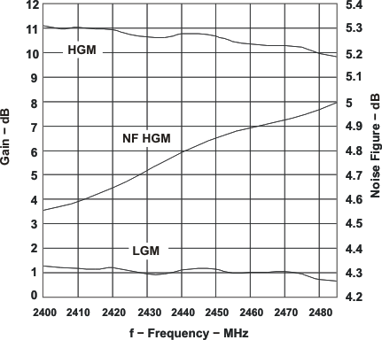 Figure 4-1 LNA Gain and Noise Figure vs Frequency
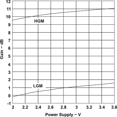 Figure 4-3 LNA Gain vs Power Supply
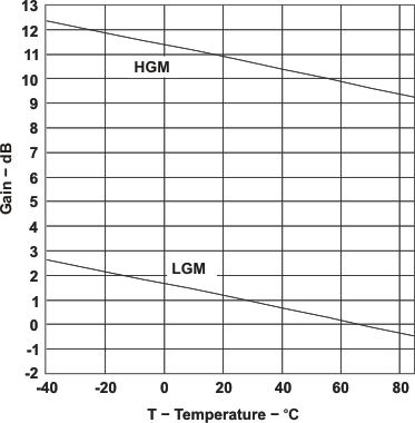 Figure 4-2 LNA Gain vs Temperature