SWRS070B March 2008 – September 2014 CC2591
PRODUCTION DATA.
3 Terminal Configuration and Functions
The CC2591 pinout and description are shown in Figure 3-1 and Table 3-1, respectively.
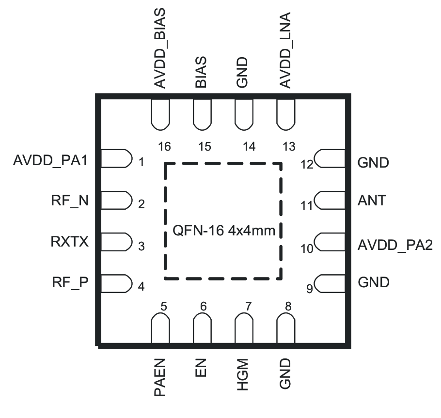 Figure 3-1 PIN AND I/O CONFIGURATION (TOP VIEW)
NOTE
The exposed die attach pad must be connected to a solid ground plane as this is the primary ground connection for the chip. Inductance in vias to the pad should be minimized. It is highly recommended to follow the reference layout. Changes will alter the performance.
For best performance, minimize the length of the ground vias, by using a 4-layer PCB with ground plane as layer 2 when CC2591 is mounted onto layer 1.
3.1 Pin Attributes
Table 3-1 Pin Attributes
| TERMINAL | TYPE | DESCRIPTION | |
|---|---|---|---|
| NO. | NAME | ||
| — | GND | Ground | The exposed die attach pad must be connected to a solid ground plane. See CC2591EM reference design for recommended layout. |
| 1 | AVDD_PA1 | Power | 2.0 V – 3.6 V Power. PCB trace to this pin serves as inductive load to PA . See CC2591EM reference design for recommended layout. |
| 2 | RF_N | RF | RF interface towards CC24xx or CC25xx device. |
| 3 | RXTX | Analog/Control | RXTX switching voltage when connected to CC24xx devices. See Table 5-2 and Table 5-3 for details. |
| 4 | RF_P | RF | RF interface towards CC24xx or CC25xx device |
| 5 | PAEN | Digital Input | Digital control pin. See Table 5-2 and Table 5-3 for details. |
| 6 | EN | Digital Input | Digital control pin. See Table 5-2 and Table 5-3 for details. |
| 7 | HGM | Digital Input | Digital control pin. HGM=1 → Device in High Gain Mode HGM=0 → Device in Low Gain Mode (RX only) |
| 8, 9, 12, 14 | GND | Ground | Secondary ground connections. Should be shorted to the die attach pad on the top PCB layer. |
| 10 | AVDD_PA2 | Power | 2.0 V – 3.6 V Power. PCB trace to this pin serves as inductive load to PA. See CC2591EM reference design for recommended layout. |
| 11 | ANT | RF | Antenna interface. |
| 13 | AVDD_LNA | Power | 2 V – 3.6 V Power. PCB trace to this pin serves as inductive load to LNA. See CC2591EM reference design for recommended layout. |
| 15 | BIAS | Analog | Biasing input. Resistor between this node and ground sets bias current to PAs. |
| 16 | AVDD_BIAS | Power | 2 V – 3.6 V Power. |