ZHCSK14E November 2007 – July 2019 VCA824
PRODUCTION DATA.
- 1 特性
- 2 应用
- 3 说明
- 4 修订历史记录
- 5 Device Comparison Table
- 6 Pin Configuration and Functions
-
7 Specifications
- 7.1 Absolute Maximum Ratings
- 7.2 ESD Ratings
- 7.3 Recommended Operating Conditions
- 7.4 Thermal Information
- 7.5 Electrical Characteristics: VS = ±5 V
- 7.6 Typical Characteristics: VS = ±5 V, AVMAX = 2 V/V
- 7.7 Typical Characteristics: VS = ±5 V, AVMAX = 10 V/V
- 7.8 Typical Characteristics: VS = ±5 V, AVMAX = 40 V/V
- 8 Detailed Description
- 9 Application and Implementation
- 10Power Supply Recommendations
- 11Layout
- 12器件和文档支持
- 13机械、封装和可订购信息
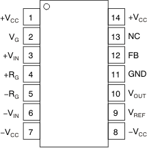
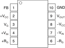
6 Pin Configuration and Functions
D Package
14-Pin SOIC
Top View

NC = No Connection
DGS Package
10-Pin VSSOP
Top View

Pin Functions
| PIN | I/O | DESCRIPTION | ||
|---|---|---|---|---|
| NAME | SOIC | VSSOP | ||
| VCC | 1,14 | 2 | P | Positive supply voltage |
| VG | 2 | 3 | I | Gain control voltage |
| +VIN | 3 | 4 | I | noninverting input |
| +RG | 4 | 5 | I | Gain set resistor noninverting input |
| –RG | 5 | 6 | I | Gain set resistor inverting input |
| –VIN | 6 | 7 | I | Inverting input |
| –VCC | 7,8 | 8 | P | Negative supply voltage |
| VREF | 9 | — | I | Output reference voltage (Non- Inverting input of output buffer) |
| VOUT | 10 | 9 | O | Output voltage |
| GND | 11 | 10 | P | Ground |
| FB | 12 | 1 | I | Feedback resistor (inverting input of output buffer) |
| NC | 13 | — | — | Not connected |