ZHCS846B April   2012  – June  2015 ULN2003LV

PRODUCTION DATA.  

  1. 特性
  2. 应用
  3. 说明
  4. 修订历史记录
  5. Pin Configuration and Functions
  6. Specifications
    1. 6.1 Absolute Maximum Ratings
    2. 6.2 ESD Ratings
    3. 6.3 Recommended Operating Conditions
    4. 6.4 Thermal Information
    5. 6.5 Electrical Characteristics
    6. 6.6 Switching Characteristics
    7. 6.7 Dissipation Ratings
    8. 6.8 Typical Characteristics
  7. Detailed Description
    1. 7.1 Overview
    2. 7.2 Functional Block Diagram
    3. 7.3 Feature Description
      1. 7.3.1 TTL and Other Logic Inputs
      2. 7.3.2 Input RC Snubber
      3. 7.3.3 High-Impedance Input Drivers
    4. 7.4 Device Functional Modes
  8. Application and Implementation
    1. 8.1 Application Information
    2. 8.2 Typical Application
      1. 8.2.1 Design Requirements
      2. 8.2.2 Detailed Design Procedure
      3. 8.2.3 Application Curve
    3. 8.3 System Examples
      1. 8.3.1 Max Supply Selector
      2. 8.3.2 Constant Current Generation
      3. 8.3.3 Unipolar Stepper Motor Driver
      4. 8.3.4 NOR Logic Driver
      5. 8.3.5 1.8-V Relay Driver
  9. Power Supply Recommendations
  10. 10Layout
    1. 10.1 Layout Guidelines
    2. 10.2 Layout Example
    3. 10.3 On-Chip Power Dissipation
    4. 10.4 Thermal Considerations
      1. 10.4.1 Improving Package Thermal Performance
  11. 11器件和文档支持
    1. 11.1 社区资源
    2. 11.2 商标
    3. 11.3 静电放电警告
    4. 11.4 Glossary
  12. 12机械、封装和可订购信息

封装选项

机械数据 (封装 | 引脚)
散热焊盘机械数据 (封装 | 引脚)
订购信息

5 Pin Configuration and Functions

D or PW Package
16-Pin SOIC or TSSOP
Top View
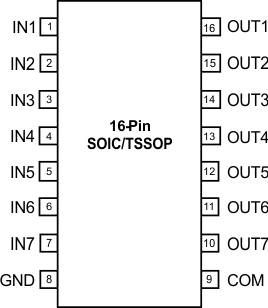
ULN2003LV po_lrs059.gif

Pin Functions

PIN TYPE DESCRIPTION
NAME NO.
IN1 1 Input Logic Input Pins IN1 through IN7
IN2 2 Input
IN3 3 Input
IN4 4 Input
IN5 5 Input
IN6 6 Input
IN7 7 Input
GND 8 Ground Ground Reference Pin
COM 9 Output Internal Free-Wheeling Diode Common Cathode Pin
OUT7 10 Output Channel Output Pins OUT7 through OUT1
OUT6 11 Output
OUT5 12 Output
OUT4 13 Output
OUT3 14 Output
OUT2 15 Output
OUT1 16 Output