ZHCSC55A January 2014 – March 2014 UCD9244-EP
PRODUCTION DATA.
- 1 特性
- 2 应用范围
- 3 说明
- 4 修订历史记录
- 5 说明(继续)
- 6 Terminal Configuration and Functions
-
7 Specifications
- 7.1 Absolute Maximum Ratings
- 7.2 Handling Ratings
- 7.3 Recommended Operating Conditions
- 7.4 Thermal Information
- 7.5 Electrical Characteristics
- 7.6 Electrical Characteristics (Continued)
- 7.7 ADC Monitoring Intervals And Response Times
- 7.8 Hardware Fault Detection Latency
- 7.9 PMBus/SMBus/I2C
- 7.10 I2C/SMBus/PMBus Timing Requirements
- 7.11 Typical Characteristics
-
8 Detailed Description
- 8.1 Overview
- 8.2 Functional Block Diagram
- 8.3
Feature Description
- 8.3.1 PMBus Interface
- 8.3.2 Resistor Programmed PMBus Address Decode
- 8.3.3 VID Interface
- 8.3.4 Jtag Interface
- 8.3.5 Bias Supply Generator (Shunt Regulator Controller)
- 8.3.6 Power-On Reset
- 8.3.7 External Reset
- 8.3.8 ON_OFF_CONFIG
- 8.3.9 Output Voltage Adjustment
- 8.3.10 Calibration
- 8.3.11 Analog Front End (AFE)
- 8.3.12 Voltage Sense Filtering
- 8.3.13 DPWM Engine
- 8.3.14 Rail/Power Stage Configuration
- 8.3.15 DPWM Phase Synchronization
- 8.3.16 Output Current Measurement
- 8.3.17 Current Sense Input Filtering
- 8.3.18 Over-Current Detection
- 8.3.19 Input Voltage Monitoring
- 8.3.20 Input UV Lockout
- 8.3.21 Temperature Monitoring
- 8.3.22 Auxiliary ADC Input Monitoring
- 8.3.23 Soft Start, Soft Stop Ramp Sequence
- 8.3.24 Non-Volatile Memory Error Correction Coding
- 8.3.25 Data Logging
- 8.4 Device Functional Modes
- 9 Applications and Implementation
- 10Power Supply Recommendations
- 11Layout
- 12Device and Documentation Support
- 13Mechanical, Packaging, and Orderable Information
9 Applications and Implementation
9.1 Application Information
9.1.1 Automatic System Identification (Auto-ID™)
By using digital circuits to create the control function for a switch-mode power supply, additional features can be implemented. One of those features is the measurement of the open loop gain and stability margin of the power supply without the use of external test equipment. This capability is called automatic system identification or Auto-ID™. To identify the frequency response, the UCD9244 internally synthesizes a sine wave signal and injects it into the loop at the Vref DAC. This signal excites the system, and the closed-loop response to that excitation can be measured at another point in the loop. The UCD9244 measures the response to the excitation at the output of the digital compensator. From the closed-loop response, the open-loop transfer function is calculated. The open-loop transfer function may be calculated from the closed-loop response.
Note that since the compensator and DPWM are digital, their transfer functions are known exactly and can be divided out of the measured open-loop gain. In this way the UCD9244 can accurately measure the power stage/load plant transfer function in situ (in place), on the factory floor or in an end equipment application and send the measurement data back to a host through the PMBus interface without the need for external test equipment. Details of the Auto-ID™ PMBus measurement commands can be found in the UCD92xx PMBus Command Reference (SLUU337).
9.2 Typical Applications
Figure 17 shows the UCD9244 power supply controller as part of a system that provides the regulation of two independent power supplies. The loop for each power supply is created by the respective voltage outputs feeding into the differential voltage error ADC (EADC) inputs, and completed by DPWM outputs feeding into the gate drivers for each power stage.
The ±Vsense rail signals must be routed to the EAp/EAn input that matches the DPWM number that controls the output power stage. For example, the power stage driven by DPWM1A must have its feedback routed to EAP1 and EAN1.
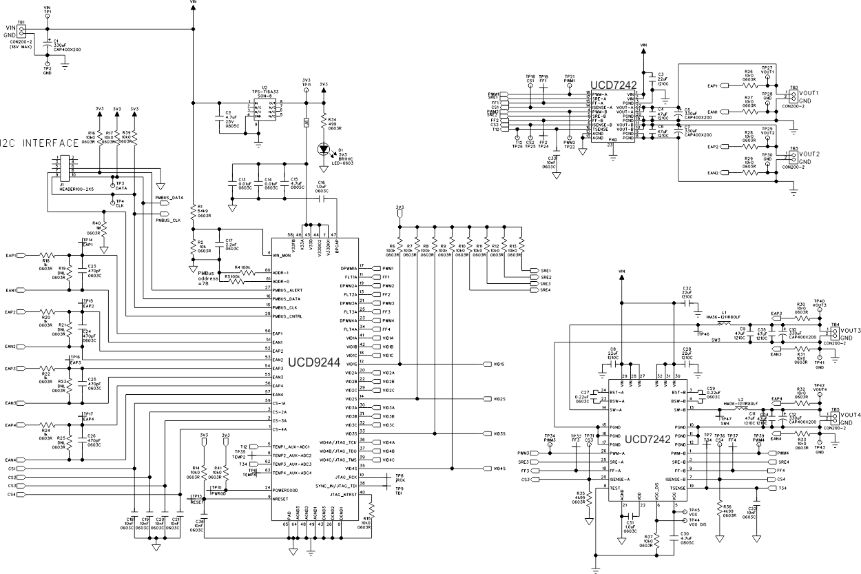 Figure 17. Typical Application Schematic
9.2.1 Design Requirements
| DESIGN PARAMETER | APPROXIMATE | UNITS | |
|---|---|---|---|
| LOWER BOUND | UPPER BOUND | ||
| KDC | 60 | 103 | dB |
| FZ | 3 kHz | Fsw/5 | kHz |
| QZ | 0.1 | 5.0 | n/a |
9.2.2 Detailed Design Procedure
9.2.2.1 Digital Compensator
Each voltage rail controller in the UCD9244 includes a digital compensator. The compensator consists of a nonlinear gain stage, followed by a digital filter consisting of a second order infinite impulse response (IIR) filter section cascaded with a first order IIR filter section.
The Texas Instruments Fusion Digital Power™ Designer development tool can be used to assist in defining the compensator coefficients. The design tool allows the compensator to be described in terms of the pole frequencies, zero frequencies and gain desired for the control loop. In addition, the Fusion Digital Power™ Designer can be used to characterize the power stage so that the compensator coefficients can be chosen based on the total loop gain for each feedback system. The coefficients of the filter sections are generated through modeling the power stage and load.
Additionally, the UCD9244 has three banks of filter coefficients: Bank-0 is used during the soft start/stop ramp or tracking; Bank-1 is used while in regulation mode; and Bank-2 is used when the measured output current is below the configured light load threshold.
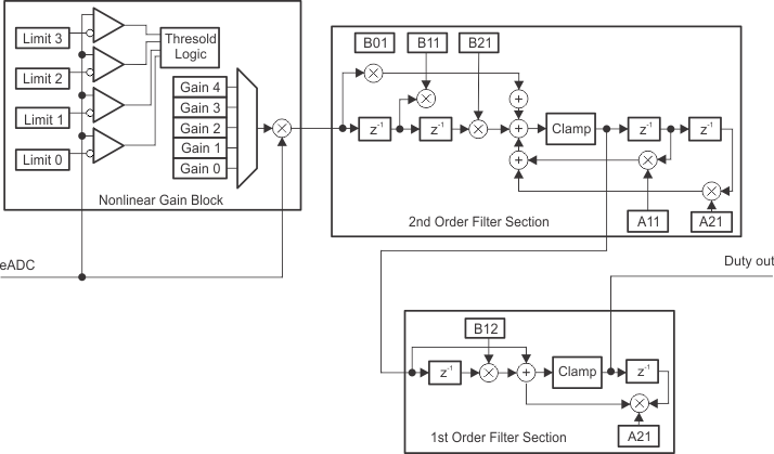 Figure 18. Digital Compensator
To calculate the values of the digital compensation filter continuous-time design parameters KDC, FZ ands QZ are entered into the Fusion Digital Power Designer software (or it calculates them automatically). Where the compensating filter transfer function is

There are approximate limits the design parameters KDC, FZ ands QZ. Though design parameters beyond these upper a lower bounds can be used to calculate the discrete-time filter coefficients, there will be significant round-off error when the continuous-time floating-point design parameters are converted to the discrete-time fixed-point integer coefficients to be downloaded to the controller.
The nonlinear gain block allows a different gain to be applied to the system when the error voltage deviates from zero. Typically Limit 0 and Limit 1 would be configured with negative values between –1 and –32 and Limit 2 and Limit 3 would be configured with positive values between 1 and 31. However, the gain thresholds do not have to be symmetrical. For example, the four limit registers could all be set to positive values causing the Gain 0 value to set the gain for all negative errors and a nonlinear gain profile would be applied to only positive error voltages.
The cascaded 1st order filter section is used to generate the third zero and third pole.