ZHCSC55A January 2014 – March 2014 UCD9244-EP
PRODUCTION DATA.
- 1 特性
- 2 应用范围
- 3 说明
- 4 修订历史记录
- 5 说明(继续)
- 6 Terminal Configuration and Functions
-
7 Specifications
- 7.1 Absolute Maximum Ratings
- 7.2 Handling Ratings
- 7.3 Recommended Operating Conditions
- 7.4 Thermal Information
- 7.5 Electrical Characteristics
- 7.6 Electrical Characteristics (Continued)
- 7.7 ADC Monitoring Intervals And Response Times
- 7.8 Hardware Fault Detection Latency
- 7.9 PMBus/SMBus/I2C
- 7.10 I2C/SMBus/PMBus Timing Requirements
- 7.11 Typical Characteristics
-
8 Detailed Description
- 8.1 Overview
- 8.2 Functional Block Diagram
- 8.3
Feature Description
- 8.3.1 PMBus Interface
- 8.3.2 Resistor Programmed PMBus Address Decode
- 8.3.3 VID Interface
- 8.3.4 Jtag Interface
- 8.3.5 Bias Supply Generator (Shunt Regulator Controller)
- 8.3.6 Power-On Reset
- 8.3.7 External Reset
- 8.3.8 ON_OFF_CONFIG
- 8.3.9 Output Voltage Adjustment
- 8.3.10 Calibration
- 8.3.11 Analog Front End (AFE)
- 8.3.12 Voltage Sense Filtering
- 8.3.13 DPWM Engine
- 8.3.14 Rail/Power Stage Configuration
- 8.3.15 DPWM Phase Synchronization
- 8.3.16 Output Current Measurement
- 8.3.17 Current Sense Input Filtering
- 8.3.18 Over-Current Detection
- 8.3.19 Input Voltage Monitoring
- 8.3.20 Input UV Lockout
- 8.3.21 Temperature Monitoring
- 8.3.22 Auxiliary ADC Input Monitoring
- 8.3.23 Soft Start, Soft Stop Ramp Sequence
- 8.3.24 Non-Volatile Memory Error Correction Coding
- 8.3.25 Data Logging
- 8.4 Device Functional Modes
- 9 Applications and Implementation
- 10Power Supply Recommendations
- 11Layout
- 12Device and Documentation Support
- 13Mechanical, Packaging, and Orderable Information
7 Specifications
7.1 Absolute Maximum Ratings(1)
over operating free-air temperature range (unless otherwise noted)| VALUE | UNIT | |
|---|---|---|
| Voltage applied at V33D to DGND | –0.3 to 3.8 | V |
| Voltage applied at V33A to AGND | –0.3 to 3.8 | V |
| Voltage applied to any terminal(2) | –0.3 to 3.8 | V |
| Maximum junction temperature (TJ) | 150 | °C |
7.2 Handling Ratings
| MIN | MAX | UNIT | ||
|---|---|---|---|---|
| Tstg | Storage temperature range | -55 | 150 | °C |
7.3 Recommended Operating Conditions
over operating free-air temperature range (unless otherwise noted)| MIN | NOM | MAX | UNIT | ||
|---|---|---|---|---|---|
| V | Supply voltage during operation, V33D, V33DIO, V33A | 3 | 3.3 | 3.6 | V |
| TJ | Operating junction temperature range | –55 | 125 | °C | |
7.4 Thermal Information
| THERMAL METRIC(1) | UCD9244-EP | UNIT | |
|---|---|---|---|
| QFN | |||
| 64 TERMINAL | |||
| θJA | Junction-to-ambient thermal resistance(2) | 24.6 | °C/W |
| θJCtop | Junction-to-case (top) thermal resistance(3) | 10 | |
| θJB | Junction-to-board thermal resistance(4) | 4.2 | |
| ψJT | Junction-to-top characterization parameter(5) | 0.2 | |
| ψJB | Junction-to-board characterization parameter(6) | 4.1 | |
| θJCbot | Junction-to-case (bottom) thermal resistance(7) | 1 | |
7.5 Electrical Characteristics
over operating free-air temperature range (unless otherwise noted)| TEST CONDITIONS | MIN | NOM | MAX | UNIT | ||
|---|---|---|---|---|---|---|
| SUPPLY CURRENT | ||||||
| IV33A | Supply current | V33A = 3.3 V | 8 | 15 | mA | |
| IV33DIO | V33DIO = 3.3 V | 42 | 55 | mA | ||
| IV33 | Total V33 supply current, V33A = V33DIO = 3.3 V | 54 | 80 | mA | ||
| IV33DIO | V33D = 3.3 V storing configuration parameters in flash memory | 52 | 65 | mA | ||
| INTERNAL REGULATOR CONTROLLER INPUTS/OUTPUTS | ||||||
| V33 | 3.3-V linear regulator | Emitter of NPN transistor | 3.25 | 3.3 | 3.6 | V |
| V33FB | 3.3-V linear regulator feedback | 4 | 4.6 | V | ||
| IV33FB | Series pass base drive | VIN = 12 V | 0.2 | 0.4 | 8 | mA |
| Beta | Series NPN pass device | 40 | ||||
| EXTERNALLY SUPPLIED 3.3 V POWER | ||||||
| V33D, V33DIO1, V33DIO2 | Digital 3.3-V power | TJ = 25°C | 3.0 | 3.6 | V | |
| V33A | Analog 3.3-V power | TJ = 25°C | 3.0 | 3.6 | V | |
| ERROR AMPLIFIER INPUTS EAPn, EANn | ||||||
| VCM | Common mode voltage each terminal | 0 | 1.8 | V | ||
| VERROR | Internal error Voltage range | AFE_GAIN field of CLA_GAINS = 1X(1) | –256 | 248 | mV | |
| EAP-EAN | Error voltage digital resolution | AFE_GAIN field of CLA_Gains = 8X | 1 | mV | ||
| REA | Input Impedance | Ground reference, TJ = 25°C | 1.5 | MΩ | ||
| IOFFSET | Input offset current | 1-kΩ source impedance,TJ = 25°C | –5 | 5 | µA | |
| Vref 10-bit DAC | ||||||
| Vref | Reference Voltage Setpoint | 0 | 1.7 | V | ||
| Vrefres | Reference Voltage Resolution | 1.56 | mV | |||
| ANALOG INPUTS CS1A, CS2A, CS3A, CS4A,VinMon, Temp1, Temp2, Temp3, Temp4, Addr0, Addr1 | ||||||
| VADC_RANGE | Measurement range for voltage monitoring | Inputs: VinMon, Temp1, Temp2, Temp3, Temp4, CS1A, CS2A, CS3A, CS4A | 0 | 2.6 | V | |
| Voffset | input offset voltage | –27 | 27 | mV | ||
| VOC_THRS | Over-current comparator threshold voltage range(2) | Inputs: CS1A, CS2A, CS3A, CS4A | 0.032 | 2 | V | |
| VOC_RES | Over-current comparator threshold voltage range | Inputs: CS, 1A, CS2A, CS3A, CS4A | 31.25 | mV | ||
| Tempinternal | Int. temperature sense accuracy | Over range from 0°C to 100°C | –15 | 15 | °C | |
| INL | ADC integral nonlinearity | TJ = -40°C to 125°C | –2.5 | 2.5 | mV | |
| Ilkg | Input leakage current | 3V applied to terminal | 100 | nA | ||
| RIN | Input impedance | Ground reference | 8 | MΩ | ||
| CIN | Current Sense Input capacitance | 10 | pF | |||
7.6 Electrical Characteristics (Continued)
over operating free-air temperature range (unless otherwise noted)| PARAMETER | TEST CONDITIONS | MIN | NOM | MAX | UNIT | |
|---|---|---|---|---|---|---|
| DIGITAL INPUTS/OUTPUTS | ||||||
| VOL | Low-level output voltage | IOL = 6 mA(1), V33DIO = 3 V | Dgnd +0.3 | V | ||
| VOH | High-level output voltage | IOH = -6 mA(2), V33DIO = 3 V | V33DIO –0.6V |
V | ||
| VIH | High-level input voltage | V33DIO = 3V | 2.1 | 3.6 | V | |
| VIL | Low-level input voltage | V33DIO = 3.5 V | 1.4 | V | ||
| SYSTEM PERFORMANCE | ||||||
| VRESET | Voltage where device comes out of reset | V33D terminal | 2.3 | 2.4 | V | |
| tRESET | Pulse width needed for reset | nRESET terminal | 2 | µs | ||
| VRefAcc | Setpoint Reference Accuracy | Vref commanded to be 1V, at 25°C AFEgain = 4, 1V input to EAP/N measured at output of the EADC(3) |
–10 | 10 | mV | |
| Setpoint Reference Accuracy over temperature | –55°C to 125°C | –40 | 40 | mV | ||
| VDiffOffset | Differential offset between gain settings | AFEgain = 4 compared to AFEgain = 1, 2, or 8 |
–4 | 4 | mV | |
| tDelay | Digital Compensator Delay | 240 | 240 + 1 switching cycle | ns | ||
| FSW | Switching Frequency | 15.260 | 2000 | kHz | ||
| Accuracy | –5% | 5% | ||||
| Duty | Max and Min Duty Cycle | 0% | 100% | |||
| V33Slew | Minimum V33 slew rate | V33 slew rate between 2.3V and 2.9V, TJ = -40°C to 125°C |
0.25 | V/ms | ||
| tretention | Retention of configuration parameters(6) | TJ = 25 °C | 100 | Years | ||
| Write_Cycles | Number of nonvolatile erase/write cycles | TJ = 25 °C | 20 | K cycles | ||
| RateVID | Max VID message rate | All rails configured to accept VID messages(5) | 1 | msg/msec | ||
| All rails configured to accept 6-bit VID messages(5) | 4 | |||||
| All rails configured to accept 8-bit VID messages(4) | 4 | |||||
7.7 ADC Monitoring Intervals And Response Times
The ADC operates in a continuous conversion sequence that measures each rail's output voltage and output current, plus six other variables (input voltage, internal temperature, and four external temperature sensors). The length of the sequence is determined by the number of output rails (NumRails) configured for use. The time to complete the monitoring sampling sequence is give by the formula: tADC_SEQ = tADC × (2 × NumRAILS + 6)
| PARAMETER | TEST CONDITIONS | MIN | TYP | MAX | UNIT | |
|---|---|---|---|---|---|---|
| tADC | ADC single-sample time | 3.84 | µs | |||
| tADC_SEQ | ADC sequencer interval | Min = 2 × 1 Rail + 6 = 8 samples Max = 2 × 4 Rails + 6 = 14 samples |
30.72 | 53.76 | µs | |
The most recent ADC conversion results are periodically converted into the proper measurement units (volts, amperes, degrees), and each measurement is compared to its corresponding fault and warning limits. The monitoring operates asynchronously to the ADC, at intervals shown in the table below.
| PARAMETER | TEST CONDITIONS | MIN | TYP | MAX | UNIT | |
|---|---|---|---|---|---|---|
| tVout | Output voltage monitoring interval | 200 | µs | |||
| tIout | Output current monitoring interval | 200×NRails | µs | |||
| tVin | Input voltage monitoring interval | 1 | ms | |||
| tTEMP | Temperature monitoring interval | 100 | ms | |||
| tAUXADC | Auxiliary ADC monitoring interval | 100 | ms | |||
Because the ADC sequencer and the monitoring comparisons are asynchronous to each other, the response time to a fault condition depends on where the event occurs within the monitoring interval and within the ADC sequence interval. Once a fault condition is detected, some additional time is required to determine the correct action based on the FAULT_RESPONSE code, and then to perform the appropriate response. The following table lists the worse-case fault response times.
| PARAMETER | TEST CONDITIONS | TYP | MAX no VID |
MAX /w VID(3) |
UNIT | |
|---|---|---|---|---|---|---|
| tOVF, tUVF | Over-/under-voltage fault response time during normal operation | Normal regulation, no PMBus activity, 4 stages enabled |
250 | 800 | µs | |
| tOVF, tUVF | Over-/under-voltage fault response time, during data logging | During data logging to nonvolatile memory(1) | 800 | 1000 | µs | |
| tOVF, tUVF | Over-/under-voltage fault response time, when tracking or sequencing enable | During tracking and soft-start ramp. | 400 | µs | ||
| tOCF, tUCF | Over-/under-current fault response time during normal operation | Normal regulation, no PMBus activity, 4 stages enabled 75% to 125% current step(2) |
100 + (600 × NRails) |
5000 | µs | |
| tOCF, tUCF | Over-/under-current fault response time, during data logging | During data logging to nonvolatile memory 75% to 125% current step | 600 + (600 × NRails) |
5000 | µs | |
| tOTF | Over-temperature fault response time | Temperature rise of 10°C/sec, at OT threshold | 1.60 | sec | ||
| t3-State | Time to tristate the PWM output after a shutdown is initiated | DRIVER_CONFIG = 0x01 | 5.5 | µs | ||
7.8 Hardware Fault Detection Latency
The controller contains hardware fault detection circuits that are independent of the ADC monitoring sequencer.
| PARAMETER | TEST CONDITIONS | MAX TIME | UNIT | |
|---|---|---|---|---|
| tFAULT | Time to disable DPWM output base on active FAULT terminal signal | High level on FAULT terminal | 18 | µs |
| tCLF | Time to disable the DPWM A output based on internal analog comparator | Step change in CS voltage from 0V to 2.5V | 4 | Switch Cycles |
7.9 PMBus/SMBus/I2C
The timing characteristics and timing diagram for the communications interface that supports I2C, SMBus and PMBus are shown below.
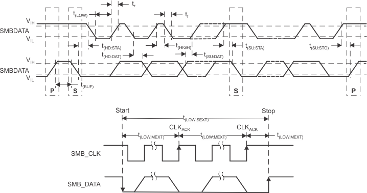 Figure 1. I2C/SMBus/PMBus Timing In Extended Mode Diagram
7.10 I2C/SMBus/PMBus Timing Requirements
TJ = –55°C to 125°C, 3V < V33 < 3.6V, typical values at TJ = 25°C| PARAMETER | TEST CONDITIONS | MIN | TYP | MAX | UNIT | |
|---|---|---|---|---|---|---|
| fSMB | SMBus/PMBus operating frequency | Slave mode; SMBC 50% duty cycle | 10 | 1000 | kHz | |
| fI2C | I C operating frequency | Slave mode; SCL 50% duty cycle | 10 | 1000 | kHz | |
| t(BUF) | Bus free time between start and stop | 5 | µs | |||
| t(HD:STA) | Hold time after (repeated) start | 0.3 | µs | |||
| t(SU:STA) | Repeated start setup time | 0.3 | µs | |||
| t(SU:STO) | Stop setup time | 0.3 | µs | |||
| t(HD:DAT) | Data hold time | Receive mode | 0 | ns | ||
| t(SU:DAT) | Data setup time | 55 | ns | |||
| t(TIMEOUT) | Error signal/detect | See (1) | 35 | ms | ||
| t(LOW) | Clock low period | 0.55 | µs | |||
| t(HIGH) | Clock high period | See (2) | 0.3 | 50 | µs | |
| t(LOW:SEXT) | Cumulative clock low slave extend time | See (3) | 25 | ms | ||
| tFALL | Clock/data fall time | Rise time tRISE = VILMAX – 0.15) to (VIHMIN + 0.15), TJ = -40°C to 125°C |
1000 | ns | ||
| tRISE | Clock/data rise time | Fall time tFALL = 0.9 V33 to (VILMAX – 0.15), TJ = -40°C to 125°C |
1000 | ns | ||
7.11 Typical Characteristics
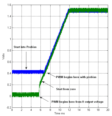 Figure 2. Soft-Start Ramp
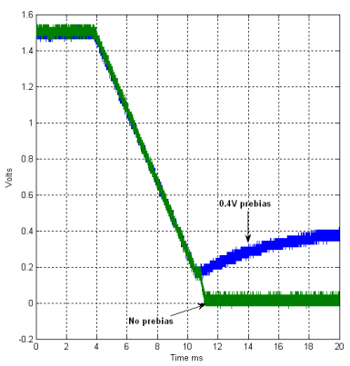 Figure 3. Soft-Stop Ramp